Method for evaluating quality of oxide semiconductor thin film and laminated body having protective film on surface of oxide semiconductor thin film, and method for managing quality of oxide semiconductor thin film

Active Publication Date: 2017-07-06
KOBE STEEL LTD
View PDF0 Cites 2 Cited by
  • Summary
  • Abstract
  • Description
  • Claims
  • Application Information

AI Technical Summary

Benefits of technology

[0041]According to the invention, the electronic state of the oxide semiconductor thin film is directly or indirectly measured, thereby the failure caused by the in-film defect in the oxide semiconductor thin film or the interfacial defect can be evaluated. Quality o

Problems solved by technology
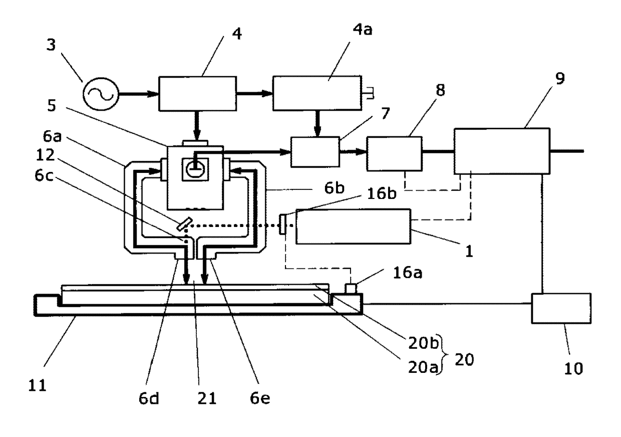
It is however known that an electron state of the oxide semiconductor thin film is varied due to a film formation step and subsequent heat treatment, affecting quality of TFT.
Hence, Vth is varied and thus a switching characteristic is disadvantageously varied.
Hence, if such light irradiation is continued in addition to application of a negative voltage (hereinafter, also referred to as “negative bias

Method used


Image

  • Method for evaluating quality of oxide semiconductor thin film and laminated body having protective film on surface of oxide semiconductor thin film, and method for managing quality of oxide semiconductor thin film
  • Method for evaluating quality of oxide semiconductor thin film and laminated body having protective film on surface of oxide semiconductor thin film, and method for managing quality of oxide semiconductor thin film
  • Method for evaluating quality of oxide semiconductor thin film and laminated body having protective film on surface of oxide semiconductor thin film, and method for managing quality of oxide semiconductor thin film

Examples


example 1-1

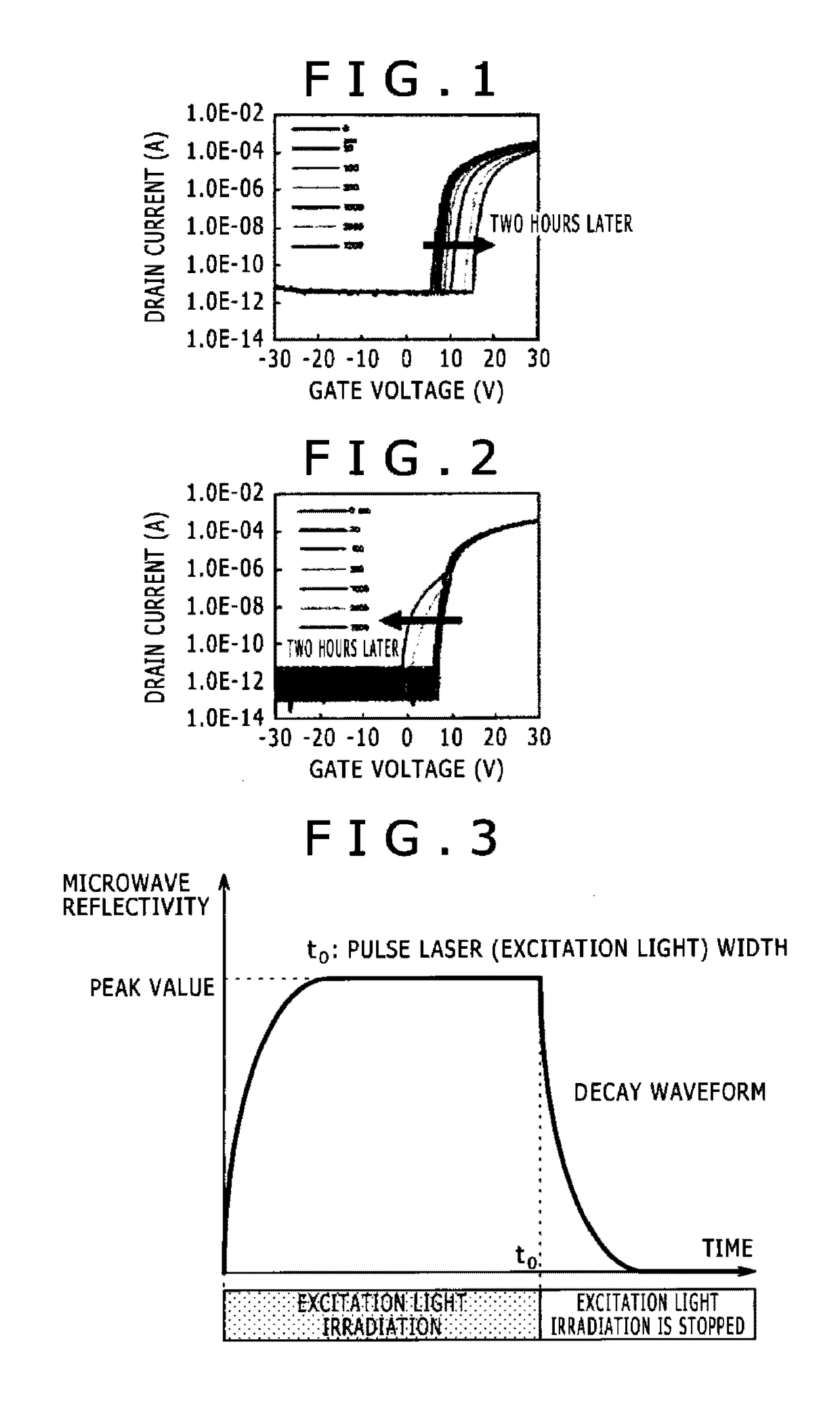
[0238]In Example 1, the following experiment was conducted to evaluate a correlation between a lifetime value calculated based on the μ-PCD method and stress resistance (ΔVth) of each of oxide semiconductor thin films (InGaZnO and IGZO herein). In this Example and Examples as described later, a reciprocal of a slope obtained by logarithmic conversion of a decay curve of reflected-wave intensity ranging from 1 / e to 1 / e2 of the maximum of the microwave reflection intensity was calculated as the lifetime value.

(1) Preparation of Sample for Lifetime Value Measurement

[0239]IGZO was deposited as an oxide semiconductor thin film on a glass substrate (EAGLE XG from Corning) having a diameter of 100 mm and a thickness of 0.7 mm by a sputtering process at the following condition.

[0240]Sputtering apparatus: “CS-200” from ULVAC, Inc.

[0241]Sputtering target composition: InGaZnO4 (In:Ga:Zn=1:1:1 (atomic ratio))

[0242]Substrate temperature: Room temperature

[0243]Thickness of oxide semiconductor thi...

example 1-2

[0282]In this Example, the following experiment was conducted to check whether the evaluation method of the invention can evaluate stress resistance during a step of forming the oxide semiconductor thin film on the previously formed gate insulating film Specifically, various samples were prepared through varying hydrogen concentration in the gate insulating film and varying gas pressure during formation of the oxide semiconductor thin film as shown in Table 2 to vary ΔVth of the oxide semiconductor thin film.

(1) Preparation of Sample for Lifetime Value Measurement

[0283]First, (i) a two-layer structure of SiO2 stacked film and (ii) a three-layer structure of SiO2 / SiN stacked film, the structures having different in-film hydrogen amounts, were each deposited as the gate insulating film on a glass substrate (EAGLE 2000 from Corning) having a diameter of 100 mm and a thickness of 0.7 mm by a plasma CVD process. Detailed formation conditions of the gate insulating films were as follows.

(...

example 1-3

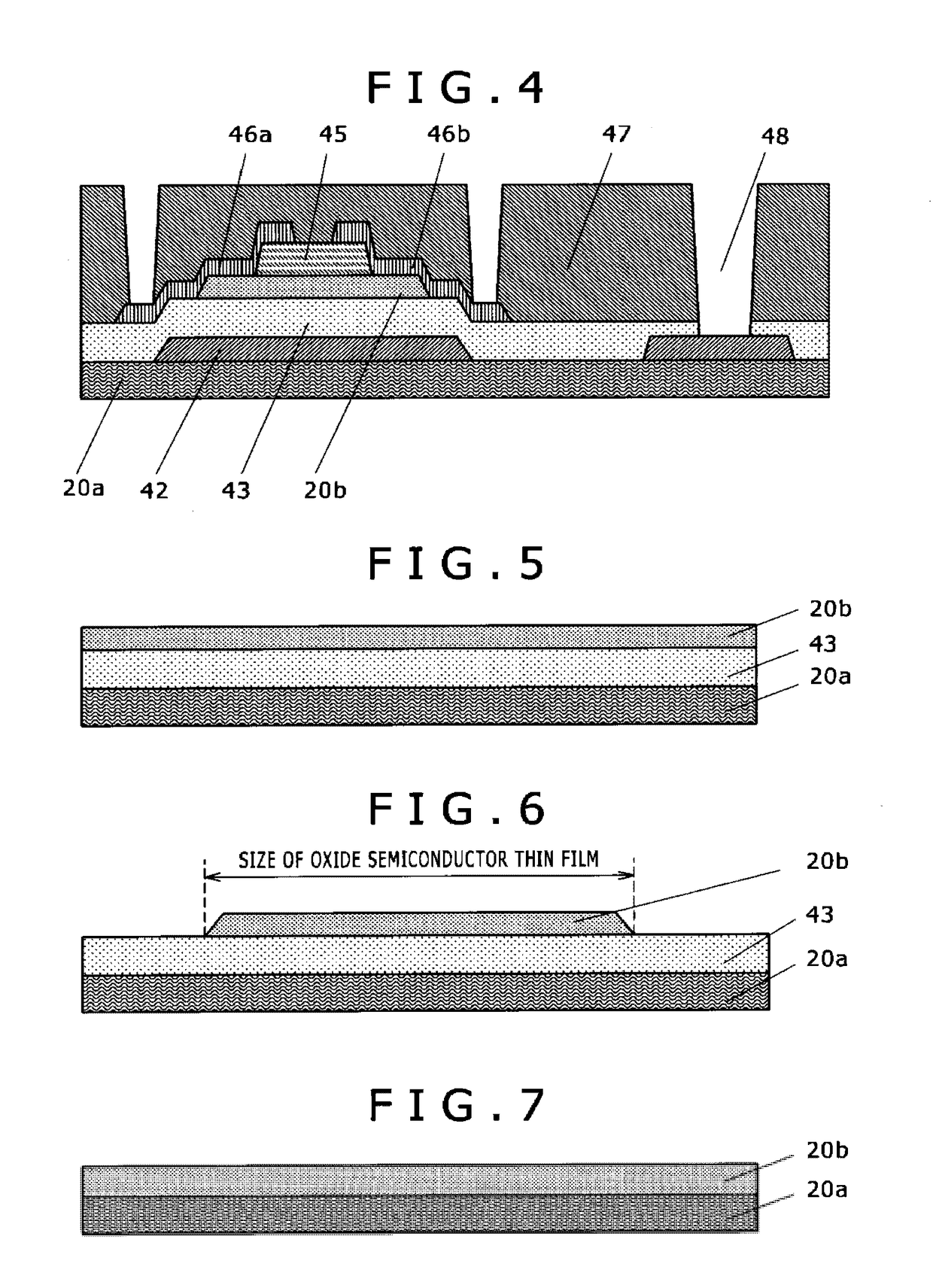
[0323]In this Example, the evaluation elements 1 to 3 illustrated in FIGS. 6, 8, and 9 were used to conduct the following experiment to check whether it is possible to evaluate stress resistance in each of the steps of:

[0324]after formation of the gate insulating film, forming the oxide semiconductor thin film on the gate insulating film (FIG. 6),

[0325]further forming the etch stop layer on the oxide semiconductor thin film (FIG. 8), and

[0326]further forming the passivation film on the etch stop layer (FIG. 9).

[0327]The evaluation element 1 in Example 1-3 is different from Example 1-2, in which the oxide semiconductor thin film is not patterned, in that the oxide semiconductor thin film is patterned.

[0328](1) Manufacturing of Element for Measurement of Lifetime Value

[0329]The following evaluation elements 1 to 3 were manufactured on a glass substrate without forming gate electrodes.

[0330]Evaluation element 1: Evaluation element of FIG. 6

[0331]Evaluation element 2: Evaluation element...


PUM


Abstract

Provided is a method for reliably and simply evaluating the quality of an oxide semiconductor thin film and a laminated body having a protective film on the surface of this oxide semiconductor thin film. Also provided is a method for reliably and simply managing the quality of an oxide semiconductor thin film. This method, which is for evaluating the quality of an oxide semiconductor thin film and a laminated body having a protective film on the surface of this oxide semiconductor thin film, has: a first step, wherein an oxide semiconductor thin film is formed on a substrate, after which the electron state of the oxide semiconductor thin film is measured by a contact method or a noncontact method, thereby evaluating defects arising from in-film defects in the oxide semiconductor thin film; and a second step, wherein the oxide semiconductor thin film is processed on the basis of a condition determined on the basis of that evaluation, after which a protective film is formed on the surface of the oxide semiconductor thin film, and then the electron state of the oxide semiconductor thin film is measured by a contact method or a noncontact method, thereby evaluating defects arising from defects at the interface between the oxide semiconductor thin film and the protective film.

Description

TECHNICAL FIELD[0001]The present invention relates to a method for evaluating quality of a laminate including an oxide for a semiconductor layer (hereinafter, referred to as “oxide semiconductor thin film”) suitable for a thin film transistor (TFT) used in a display such as a liquid crystal display or an organic EL display and a protective film on a surface of the oxide semiconductor thin film, and relates to a quality control method of the oxide semiconductor thin film. In detail, the invention relates to a technique for measuring a failure caused by an in-film defect in the oxide semiconductor thin film or a failure caused by an interfacial defect between the oxide semiconductor thin film and a protective film provided on a surface of the oxide semiconductor thin film by a contact method or a noncontact method, and evaluating quality of a laminate including the oxide semiconductor thin film, and relates to a quality control method of the oxide semiconductor thin film.BACKGROUND AR...

Claims


Application Information

Patent Timeline
IPC IPC(8): H01L21/66
CPCH01L22/14H01L22/12G01R31/2656H01L29/66969H01L29/7869H01L27/14649H01L27/1465H01L22/20H01L29/41733
Inventor KAWAKAMI, NOBUYUKIHAYASI, KAZUSHIKUGIMIYA, TOSHIHIROOCHI, MOTOTAKA
Owner KOBE STEEL LTD
Why Eureka
Try Eureka