Methods of manufacturing electrodes by in-situ electrodeposition and devices comprising said electrodes

a manufacturing method and electrode technology, applied in the field of manufacturing electrode materials by in-situ electrodeposition and devices comprising said electrodes, can solve the problems of high cost, high cost, complicated and unsuitable for many metals, and the electrodes must be handled in high vacuum, so as to increase the number of possible device configurations, enhance charge injection, and increase the reactivity to air

Inactive Publication Date: 2017-08-10
CAMBRIDGE DISPLAY TECH LTD
View PDF2 Cites 3 Cited by
  • Summary
  • Abstract
  • Description
  • Claims
  • Application Information

AI Technical Summary

Benefits of technology

[0012]Generally speaking, the present invention describes a method of manufacturing electrodes in an electronic device or a charge storage device, comprising the steps of: providing a multilayer film comprising: a electrodeposition layer formed of a plating composition comprising metal or metalloid ions and a n-type electroactive material, and a negative charge collection layer in contact with the electrodeposition layer; and subsequently electrodepositing an electrode layer in situ on a surface of the negative charge collection layer by reducing the metal or metalloid ions to a non-ionic state. Thereby, it is possible to create a low work function electrode after the device structure has been at least partly pre-assembled, so that the multilayer film may be encapsulated against air and / or liquids prior to the electrodeposition step. Thus, the method solves the problem of providing low work function material such as Zn, Mg, Ca or Li in a device without requiring complex equipment needed to handle these pure materials due to their high reactivity towards air and water. Furthermore, the method significantly expands the number of possible device configurations. Method of enhancing charge injection in an electronic device or charge storage device comprising the steps of: pre-assembling an electronic device or charge storage device, wherein the pre-assembled device comprises a electrodeposition layer formed of a plating composition comprising metal or metalloid ions and an n-type electroactive material; and subsequently applying an electric field to the electronic device or charge storage device so as to effect electrodeposition of an electrode layer in situ by reducing the metal or metalloid ions to a non-ionic state.

Problems solved by technology

However, low-work function electrode layers are usually applied by using thermal evaporation or sputtering, which is expensive, complicated and not readily applicable to many metals, such as Zn.
In addition, these electrodes must be handled in high vacuum and necessitate elaborate equipment due to the high reactivity of the pure metals towards air and water.
However, said method requires an additional manufacturing step, and it still remains difficult to achieve a work function as low as that of pure alkali metals, for example, by using this method.
However, these methods require a drying step and elaborate processing of the formed electrodes under inert gas atmosphere so as to avoid contact with air and water.
Moreover, the possible device configurations obtainable by these methods are limited in terms of electrode placement, since due to the reactivity of the electrode material towards residual solvent (e.g. water), the deposition of solution-processed layers on top of the electrode material (or alternatively the deposition of the electrode on top of a solution-processed layer) is either not possible or results in a non-uniform and deteriorated electrode layer.
However, a method of preparation of electrodes having low work function, let alone a method solving the abovementioned problems, is not disclosed.

Method used


Image

  • Methods of manufacturing electrodes by in-situ electrodeposition and devices comprising said electrodes
  • Methods of manufacturing electrodes by in-situ electrodeposition and devices comprising said electrodes
  • Methods of manufacturing electrodes by in-situ electrodeposition and devices comprising said electrodes

Examples


Embodiment Construction

Methods of In Situ Electrode Electrodeposition and Charge Injection

[0018]For a more complete understanding of the present invention, reference is now made to the following description of the illustrative embodiments thereof:

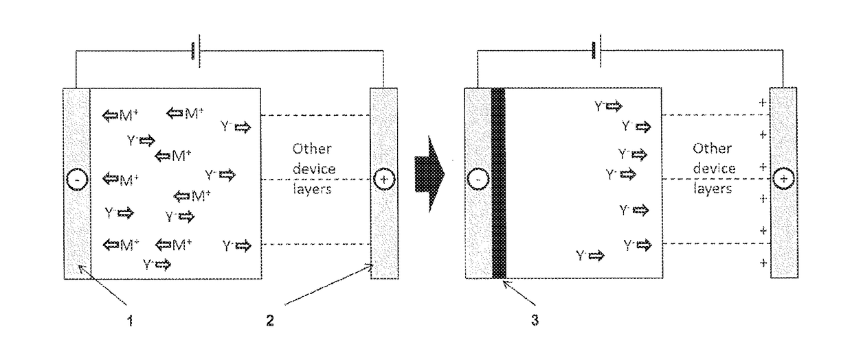
[0019]This invention describes a process for making an electrode in situ inside the device using electrodeposition and devices produced by using this process.

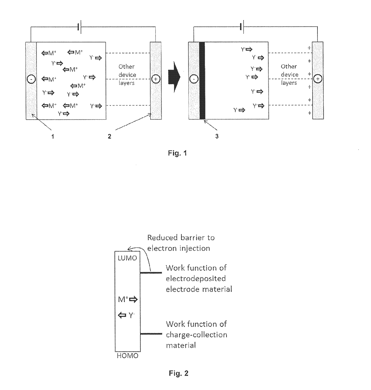
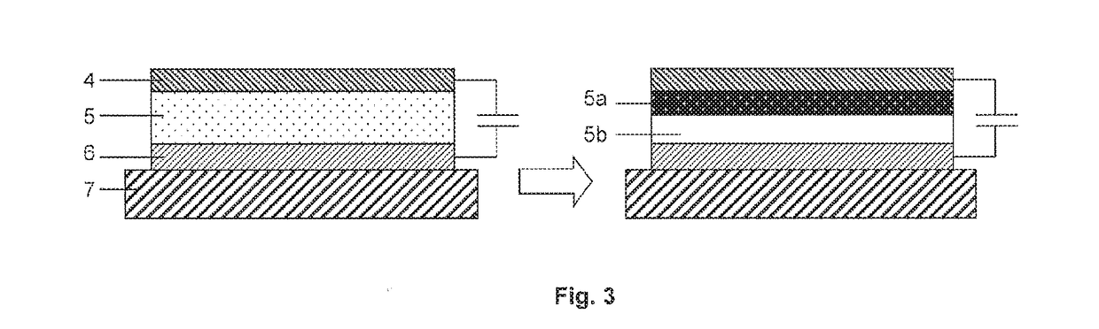
[0020]In one embodiment, the present invention relates to a method of manufacturing an electronic device or a charge storage device, comprising the steps of: providing a multilayer film comprising a electrodeposition layer formed of a plating composition comprising metal or metalloid ions and an n-type electroactive material, and a negative charge collection layer in contact with the electrodeposition layer; and subsequently electrodepositing an electrode layer in situ on a surface of the negative charge collection layer by reducing the metal or metalloid ions to a non-ionic state.

[0021]The expression “in si...


PUM

PropertyMeasurementUnit
ion conductivityaaaaaaaaaa
work functionaaaaaaaaaa
n-type semiconductiveaaaaaaaaaa

Abstract

This invention relates to a method for fabrication of electrode material in electronic devices by in situ-electrodeposition of metal or metalloid ions that are present in the device. In another aspect, the present invention relates to electronic devices and charge storage devices comprising the electrodes manufactured by said method. Furthermore, the present invention further relates to a method of enhancing charge injection in an electronic device or charge storage device comprising the steps of: pre-assembling an electronic device or charge storage device and subsequently applying an electric field to effect electrodeposition of an electrode layer in situ by reducing the metal or metalloid ions to a non-ionic state.

Description

RELATED APPLICATIONS[0001]This application claims the benefits under 35 U.S.C. §119(a)-(d) or 35 U.S.C. §365(b) of British application number 1602109.9, filed Feb. 5, 2016, the entirety of which is incorporated herein by reference.FIELD OF INVENTION[0002]This invention relates to a method for fabrication of electrode material in electronic devices by in situ-electrodeposition of metal or metalloid ions that are present in the device. In another aspect, the present invention relates to electrodes manufactured by said method and electronic and charge storage devices comprising the electrodes.BACKGROUND OF THE INVENTION[0003]A large number of charge storage devices (e.g. thin film batteries) and electronic devices (e.g. organic thin-film optoelectronic devices including organic light-emitting diodes (OLEDs), organic thin-film transistors (TFTs) or organic solar cells (OSCs)), require at least one electrode material which exhibits a work function that is sufficiently low to either injec...

Claims


Application Information

Patent Timeline
Patent Type & Authority Applications(United States)
IPC IPC(8): C25D13/02H01M4/04H01L51/52H01L51/00H01L51/56H01L51/50
CPCC25D13/02H01L51/56H01L51/5012H01L51/5032H01L51/5253H01M4/0457H01L51/5092H01L51/0021H01L51/5206H01L51/5221H01L51/5056C25D15/00Y02E60/10H10K71/60H10K50/135H10K50/81H10K50/82H10K50/844H10K71/00H01L21/44H10K10/82H10K50/11H10K50/15H10K50/171
Inventor PILLOW, JONATHAN
Owner CAMBRIDGE DISPLAY TECH LTD
Why Eureka
Try Eureka