Transparent electrode materials and methods for forming same

a technology of transparent electrodes and electrode materials, which is applied in the direction of conductive materials, carbon-silicon compound conductors, metal/alloy conductors, etc., can solve the problems of poor performance, inability to extract current from the active surface of the electrode, and inacceptable sheet resistance, so as to increase the transfer effect, lower and the resistance of the sheet is higher.

Inactive Publication Date: 2017-08-10
FLINDERS PARTNERS
View PDF5 Cites 12 Cited by
  • Summary
  • Abstract
  • Description
  • Claims
  • Application Information

AI Technical Summary

Benefits of technology

[0063]Further, the close interaction of the nanowires and nanotubes in the conductive network assists with the preferred adoption of a stamp transfer step for the formation of the nanowire / nanotube network. In a preferred form, to be suitable for a subsequent roll-to-roll electrode formation process, nanotubes are preferably co-deposited with nanowires to increase the efficacy of transfer to a planar template substrate during electrode fabrication. Without the presence of the nanotubes, the nanowires form a dense network after transfer from a cellulose ester membrane, with a somewhat higher sheet resistance suggesting that the network is not as well interconnected.
[0064]However, by co-depositing nanowires with, for example, about 20 wt % nanotubes, significantly lower sheet resistivities have been found to be achievable (such as in the range of 11 to 18Ω / □). Additionally, by utilising a stamp transfer process, the sheet resistance has been lower still and has also given rise to a lower standard deviation in sheet resistance readings, relecting better reproducibility with this preferred form of the process.

Problems solved by technology

The reason for there being any type of association between the AgNWs and the SWCNTs, in these comparative examples, has been determined to be due to a solution phase interaction between the AgNWs and SWCNTs prior to deposition onto the cellulose ester membranes, which is different to a structure obtained by the sequential deposition of nanowires followed by nanotubes, which can have poorer performance.
If a non-conductive material, such as an epoxy, were to completely cover the SWCNTs and AgNWs, current would not be extractable from the active surface of the electrode and the sheet resistance would be in the mega-ohm range and completely unacceptable.

Method used


Image

  • Transparent electrode materials and methods for forming same
  • Transparent electrode materials and methods for forming same
  • Transparent electrode materials and methods for forming same

Examples


Embodiment Construction

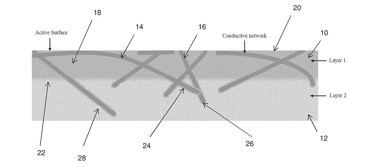
[0083]The following description outlines experimental work for the preparation of exemplary transparent electrode materials in accordance with the present invention. Specifically, exemplary transparent electrode materials of these embodiments are as illustrated in FIG. 1 and include a single conductive layer 10 and a base layer 12 that is non-conductive. The conductive layer 10 is a conductive network formed by metallic nanowires 14 and carbon nanotubes 16, which in these embodiments are the preferred silver nanowires (AgNW) and single-walled carbon nanotubes (SWCNT) encapsulated in a preferred conductive material 18.

[0084]The conductive layer has a smooth active surface 20 and a second surface 22, noting that the second surface 22 of the conductive layer 10 has encapsulated nanowires 24 and / or nanotubes 26 projecting therefrom. In this respect, the projecting nanowires and / or nanotubes are embedded in the base layer 12, and are shown to be almost completely encapsulated by the cond...


PUM

PropertyMeasurementUnit
transparencyaaaaaaaaaa
diameteraaaaaaaaaa
diameteraaaaaaaaaa

Abstract

A transparent electrode material including a conductive layer having an active surface and a second surface, and an adjacent base layer, wherein: ∘ the conductive layer includes a conductive network formed by metallic nanowires and carbon nanotubes encapsulated in a conductive material; ∘ the second surface of the conductive layer has encapsulated nanowires and/or nanotubes projecting therefrom; and ∘ the encapsulated nanowires and/or nanotubes projecting from the second surface of the conductive layer are embedded in the adjacent base layer; whereby the active surface of the conductive layer is smooth and electrically active, and the transparent electrode material has a sheet resistance less than 50 Ω/sq and a transparency greater than 70%.

Description

TECHNICAL FIELD[0001]The present invention relates to transparent electrode materials, and methods for forming those materials, the materials being suitable for use in the fabrication of optoelectronic devices (ideally flexible optoelectronic devices), and being a nanocomposite of metallic nanowires and carbon nanotubes.BACKGROUND OF INVENTION[0002]Optoelectronic devices such as flat panel displays, solar cells and light emitting diodes, and the more recently emerging technologies of organic photovoltaic devices, organic light emitting diodes, and touch screens, rely on transparent electrodes for optical transparency and conductivity. Indium tin oxide (ITO) has become the most utilized material for transparent electrodes due to its desirably low sheet resistance (15 to 60 Ω / sq) and desirably high optical transparency (>90%).[0003]In recent years, there has been increasing interest in the production of flexible electronics. Flexibility enables thin film electronics to be manufactu...

Claims


Application Information

Patent Timeline
Patent Type & Authority Applications(United States)
IPC IPC(8): H01L51/44H01B5/14H01B1/04H01B1/12H01L51/00H01B1/02
CPCH01L51/444H01L51/0021H01B5/14H01B1/04H01B1/124H01B1/02H01B1/22H01B1/24H01J1/304Y02E10/549H10K85/215H10K85/221H10K85/113H10K30/821H10K71/60
Inventor STAPLETON, ANDREW JOHNLEWIS, DAVID ANDREWSHAPTER, JOSEPH GEORGEANDERSSON, GUNTHER GEROLFQUINTON, JAMIE SCOTTELLIS, AMANDA
Owner FLINDERS PARTNERS
Why Eureka
Try Eureka