Display device and method for manufacturing the same

a technology of a display device and a manufacturing method, which is applied in the direction of semiconductor devices, basic electric elements, electrical appliances, etc., can solve the problems of not being able to meet limit conditions, not being able to reduce the current variation of each pixel, and high cost of a device and a laser material, so as to reduce the current variation, reduce the power consumption, and reduce the current variation

Active Publication Date: 2017-09-28
JAPAN DISPLAY INC
View PDF6 Cites 28 Cited by
  • Summary
  • Abstract
  • Description
  • Claims
  • Application Information

AI Technical Summary

Benefits of technology

[0010]According to another aspect of the present invention, since the first thin film transistor and the second thin film transistor are the staggered thin film transistors, the parasitic capacitance becomes small, and the drive performance is high. Since the second channel layer of the second thin film transistor is formed of the oxide semiconductor, it is possible to decrease the current variation. Furthermore, since the second thin film transistor is formed after the first thin film transistor, the second thin film transistor is not affected by the heat at the time of forming the first channel layer configured of the low-temperature polysilicon.

Problems solved by technology

The silicon is polycrystallized by excimer laser annealing, but shot variation of the laser becomes large, and it is not possible to reduce current variation of each pixel.
Therefore, there is a need to provide a correction circuit, or to repeat irradiation by irradiating the silicon with the laser several times, and there are problems such as high cost of a device and a material of the laser.
However, it is not possible to satisfy limit conditions such as a narrow frame and low power consumption with the current thin film transistor using the oxide semiconductor.

Method used


Image

  • Display device and method for manufacturing the same
  • Display device and method for manufacturing the same
  • Display device and method for manufacturing the same

Examples


first embodiment

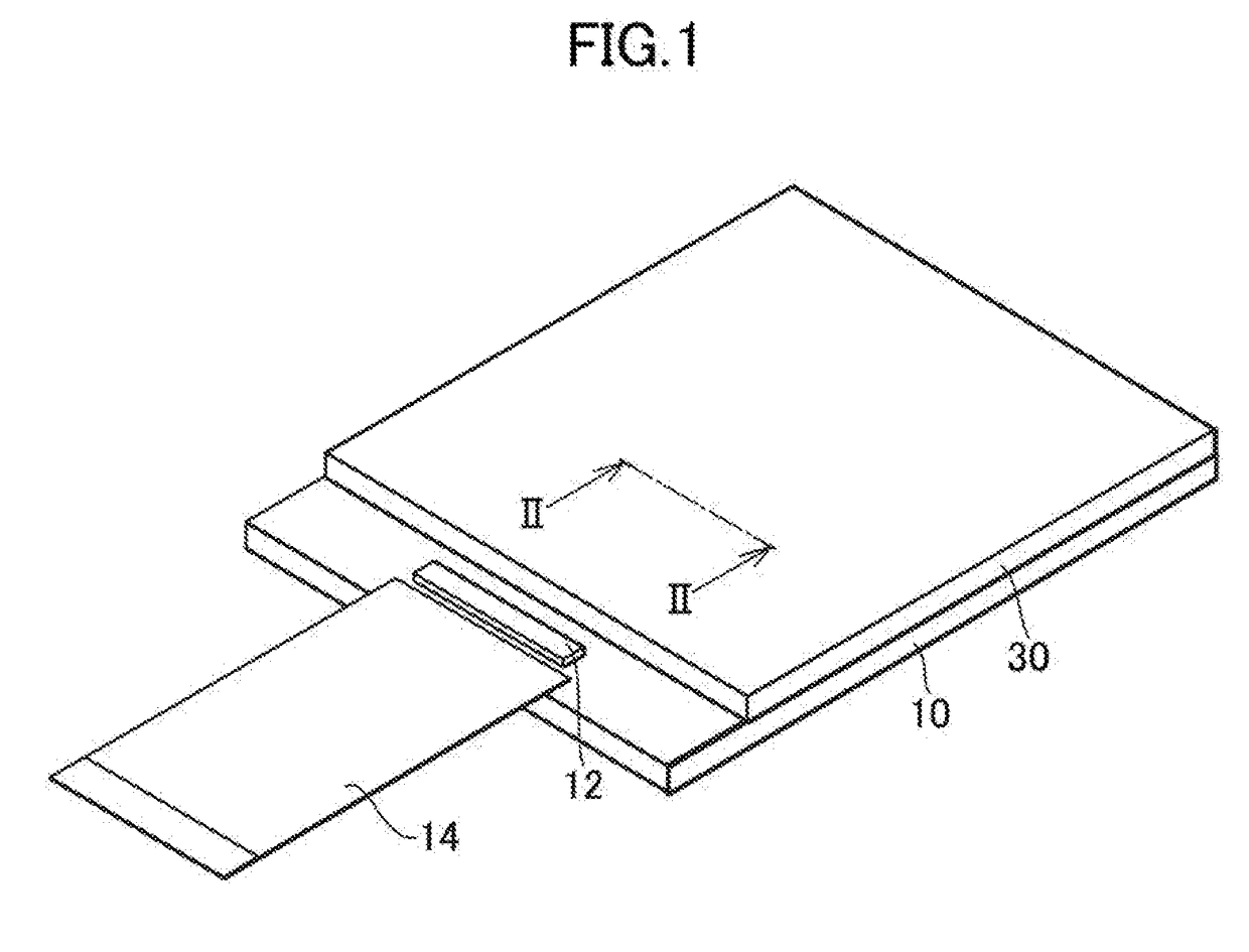
[0019]FIG. 1 is a perspective view of a display device according to a first embodiment of the present invention. As a display device, an organ electroluminescence display device is used as an example. For example, the display device combines unit pixels (sub-pixels) of a plurality of colors which are configured of red, green and blue with each other, forms a full-color pixel (pixel), and displays a full-color image. For example, the display device includes a first substrate 10 having flexibility by being configured of a resin. An integrated circuit chip 12 that drives an element for displaying the image is installed in the first substrate 10, and a flexible printed board 14 for electrical connection to the outside is connected, to the first substrate 10.

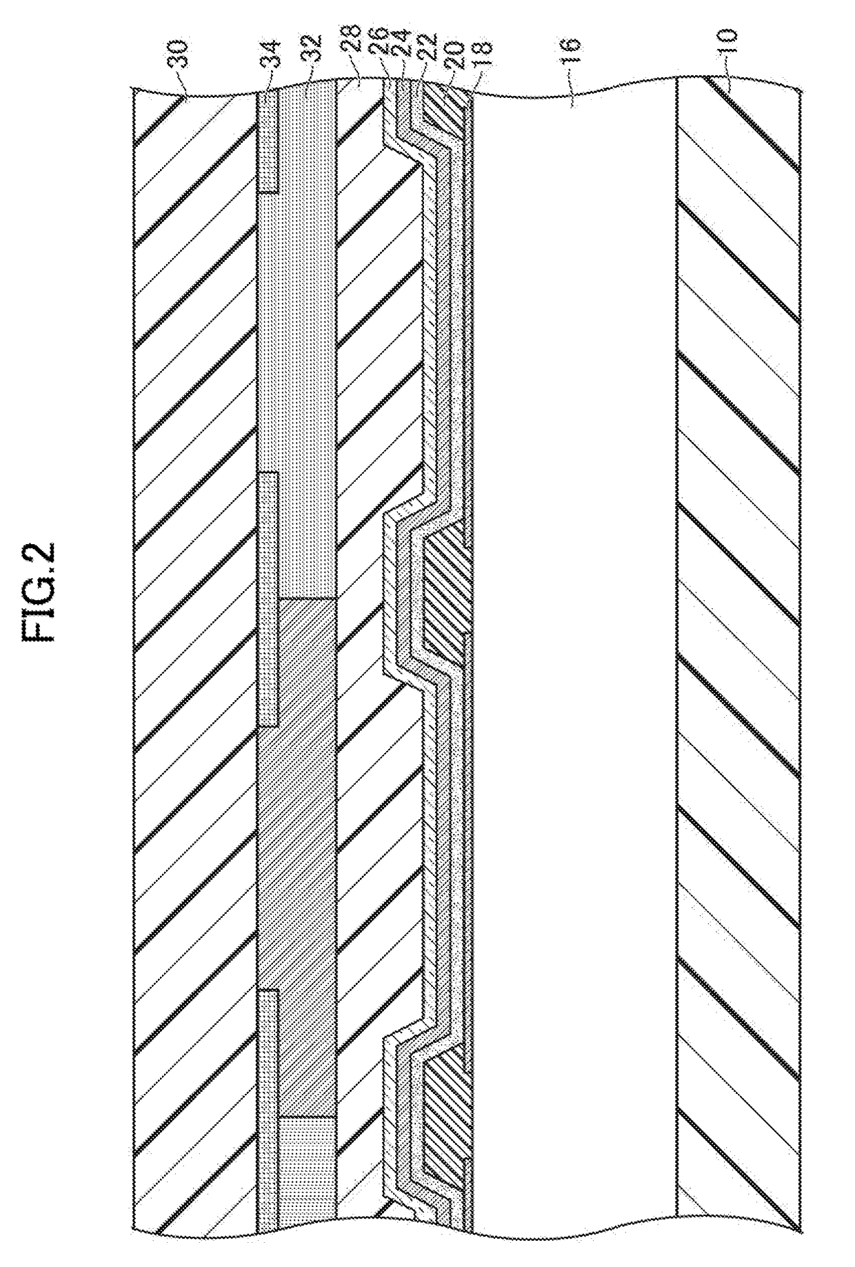
[0020]FIG. 2 is a sectional view which is taken along II-II line of the display device illustrated in FIG. 1. A circuit layer 16 is stacked on the first substrate 10. Details of the circuit layer 16 will be described later. On the ci...

modification example

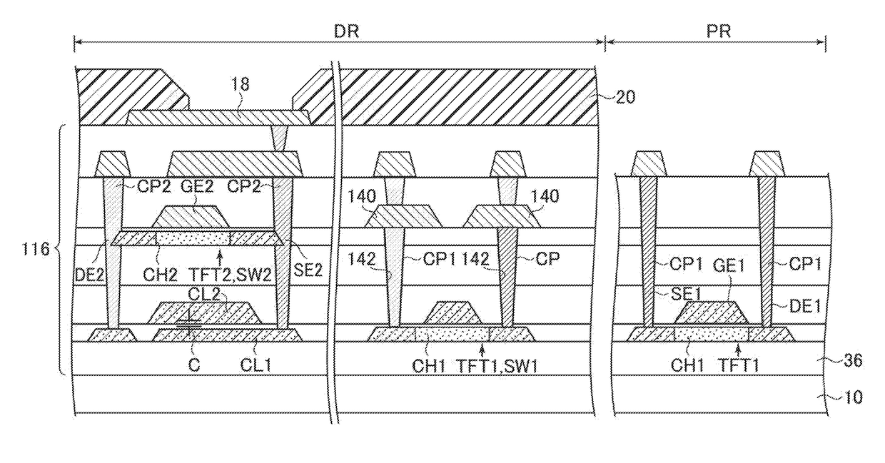
[0033]FIG. 5 is a diagram illustrating a modification example of the first embodiment. In the modification example, the plurality of thin film transistors provided in the display region DR include the first thin film transistor TFT1 at a position of the same layer as the first thin film transistor TFT1 of the peripheral region PR. That is, the first switching element SW1 illustrated in FIG. 3 is the first thin film transistor TFT1. The first contact plug CP1 that penetrates the upper insulating layer in comparison with the first thin film transistor TFT1 of a circuit layer 116, and is connected to the first channel layer CH1, is provided.

[0034]The plurality of layers configuring the circuit layer 116 include a metal layer 140 that is formed of the same material at a position of the same layer as the second gate electrode GE2 of the second thin film transistor TFT2 so as to overlap at least an end portion of the first channel layer CH1 of the first thin film transistor TFT1. The meta...

second embodiment

[0038]FIG. 6 is a circuit diagram of a display device according to a second embodiment of the present invention. In the embodiment, the video signal is written in the capacitor C by the first switching element SW1, the current flowing through the display element DE is controlled by the second switching element SW2, and a current supply is switched between an ON state and an OFF state by a third switching element SW3.

[0039]FIG. 7 is an outline diagram illustrating details of a circuit layer 216 in the second embodiment. In the embodiment, the capacitor C illustrated in FIG. 6 is configured of a plurality of capacitors (first capacitor C1, second capacitor C2 and third capacitor C3) which are connected to each other in series.

[0040]The first capacitor C1 includes a pair of electrodes E1 that is formed by injecting the ions into the low-temperature polysilicon layer. The pair of electrodes E1 is configured of the same material at the same layer as the first channel layer CH1 and the fi...


PUM


Abstract

A plurality of thin film transistors provided in a peripheral region are first staggered thin film transistors where a first channel layer configured of low-temperature polysilicon is included, and the first channel layer is not interposed between a first source electrode and a first gate electrode, and between a first drain electrode and the first gate electrode. A plurality of thin film transistors provided in a display region are second staggered thin film transistors where a second channel layer configured of an oxide semiconductor is included, and the second channel layer is not interposed between a second source electrode and a second gate electrode, and between a second drain electrode and the second gate electrode. The first thin film transistor is located below the second thin film transistor.

Description

CROSS-REFERENCE TO RELATED APPLICATION[0001]The present application claims priority from Japanese application JP2016-058455 filed on Mar. 23, 2016, the content of which is hereby incorporated by reference into this application.BACKGROUND OF THE INVENTION1. Field of the Invention[0002]The present invention relates to a display device and a method for manufacturing the same.2. Description of the Related Art[0003]A display device displays an image by emitting light with luminance and chromaticity responding to each pixel. For example, the light is emitted by flowing a current through an organic light-emitting layer provided between a plurality of pixel electrodes which are arranged in a matrix shape and a common electrode which is common to the pixel electrodes. In each of the pixels, a pixel circuit where a plurality of thin film transistors are combined with a capacitor is laid out.[0004]The thin film transistor configured of low-temperature polysilicon is frequently used since drive...

Claims


Application Information

Patent Timeline
Patent Type & Authority Applications(United States)
IPC IPC(8): H01L27/32
CPCH01L27/3262H01L27/3276H01L27/3265H01L27/1222H01L29/78675H01L27/1225H01L27/1255H01L27/124H01L2227/323H01L27/1262H01L29/66757H01L29/66969H01L29/7869H10K59/1213H10K59/1201H01L27/0688H01L27/1251H01L27/1259H10K59/12H10K59/131H10K59/1216
Inventor MARUYAMA, SATOSHI
Owner JAPAN DISPLAY INC
Why Eureka
Try Eureka