Controlling dry etch process characteristics using waferless dry clean optical emission spectroscopy

Active Publication Date: 2017-10-05
TOKYO ELECTRON LTD
View PDF8 Cites 6 Cited by
  • Summary
  • Abstract
  • Description
  • Claims
  • Application Information

AI Technical Summary

Benefits of technology

The patent is about a way to make sure that each wafer in a lot is clean and ready for processing. It uses a special technique called Optical Emission Spectroscopy (OES) to monitor the light emitted from a plasma during a dry cleaning process. This helps to determine the effectiveness of the cleaning process and can be used to adjust and optimize the cleaning process for better control over the patterned device wafers.

Problems solved by technology

One of the problems with dry etch processes for via and trench features is the variation in the etch profile during the processing of a full lot of wafers.
If these constituents are not effectively removed from the chamber to the same degree during dry clean cycles between wafers, polymer deposition can accumulate in a chamber leading to the build-up of a film layer which can lead to particle formation and peeling, and can generate defects and device failure on a wafer.
In addition, ineffective or inconsistent waferless dry cleaning (WLDC) of the chamber between device wafers, can lead to varying residual CF constituents in the chamber, which subsequently are introduced during a successive dry etch process of a device wafer that affects the uniformity of etch profile characteristics from one wafer lot to the next.

Method used


Image

  • Controlling dry etch process characteristics using waferless dry clean optical emission spectroscopy
  • Controlling dry etch process characteristics using waferless dry clean optical emission spectroscopy
  • Controlling dry etch process characteristics using waferless dry clean optical emission spectroscopy

Examples


Embodiment Construction

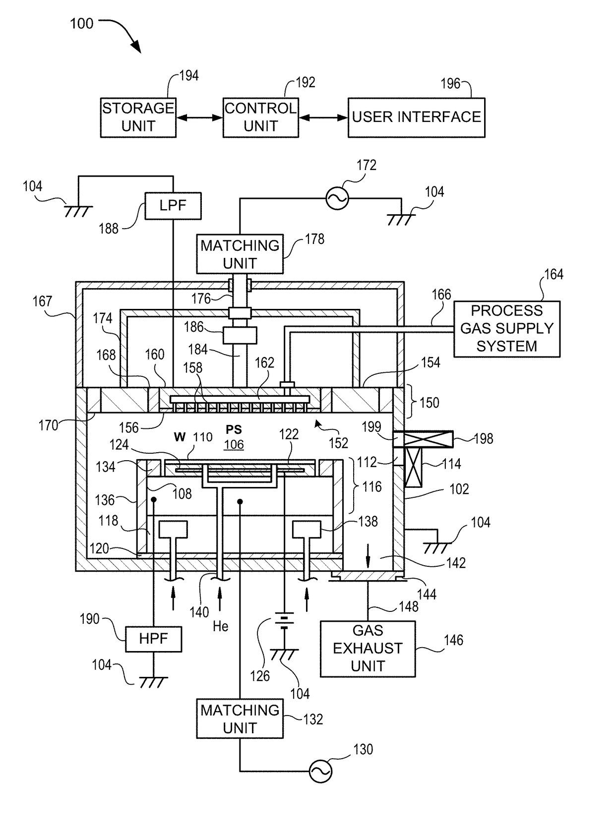
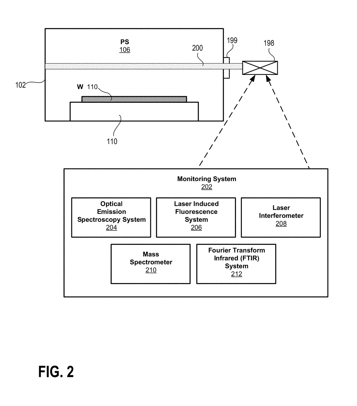
[0012]Described herein are architectures, platforms and methods for analyzing residue constituents in a waferless dry clean (WLDC) process, and in particular analysis using Optical Emission Spectroscopy (OES). A process control monitor / metric such as OES can be utilized to analyze the effectiveness of a WLDC process by evaluation of carbon (C) and fluorine (F) based wavelengths in the spectra for a batch of wafers.

[0013]Moreover, a WLDC process can be optimized based on OES spectra of undesirable residue constituents being removed by the dry cleaning process following one particular device wafer process. Typically, an ineffective WLDC process will never show the leveling out in OES intensity for the wavelength examined of a constituent that is intended to be removed by the WLDC. However, the OES spectra of this constituent would show the leveling out in intensity once the endpoint was reached for the WLDC process; this endpoint time can be utilized for determining the ideal completi...


PUM


Abstract

Described herein are architectures, platforms and methods for acquiring optical emission spectra from an optical emission spectroscopy system by flowing a dry cleaning gas into a plasma processing chamber of the plasma processing system and igniting a plasma in the plasma processing chamber to initiate the waferless dry cleaning process.

Description

RELATED APPLICATIONS[0001]This application is based on and claims priority to U.S. Provisional Patent Application No. 61 / 316,021, entitled “METHOD FOR CONTROLLING DRY ETCH PROCESS CHARACTERISTICS USING WAFERLESS DRY CLEAN OPTICAL EMISSION SPECTROSCOPY” (Ref. No. TEA-136US1-PRO), filed on Mar. 31, 2016.BACKGROUND[0002]One of the problems with dry etch processes for via and trench features is the variation in the etch profile during the processing of a full lot of wafers. This may be due to the build-up of carbon (C) and fluorine (F) (collectively referred to as CF)-based etch gas constituents used for passivation and etch selectivity, which are used to form specific etch profiles for patterned wafers in semiconductor processing. If these constituents are not effectively removed from the chamber to the same degree during dry clean cycles between wafers, polymer deposition can accumulate in a chamber leading to the build-up of a film layer which can lead to particle formation and peeli...

Claims


Application Information

Patent Timeline
IPC IPC(8): B08B7/00G01N21/94H01J37/32G01N21/73H01L21/67B08B9/08
CPCB08B7/0035H01L21/67069B08B9/0865H01J37/32146H01J2237/335H01J37/32697H01J37/32972G01N21/73G01N21/94H01J37/32669H01J37/32862H01J37/32981H01L21/02046H01L21/3065H01L21/67034H01L22/12H05H1/46H01L21/67023
Inventor COPPA, BRIAN J.VEDHACHALAM, DEEPAKDASSAPA, FRANCOIS C.
Owner TOKYO ELECTRON LTD
Why Eureka
Try Eureka