Structure and process for metal cap integration

Inactive Publication Date: 2017-10-19
IBM CORP
View PDF8 Cites 3 Cited by
  • Summary
  • Abstract
  • Description
  • Claims
  • Application Information

AI Technical Summary

Benefits of technology

[0005]In one embodiment, the disclosure relates to semiconductor structure comprising: a substrate having a cavity formed therein; a barrier material lining a portion of the cavity; a conductive material formed over the harrier material, the conductive material defining an interconnect layer; a metal cap formed over at least a portion of the conductive material; an oxygen scavenger layer formed over the metal cap layer, the ox

Problems solved by technology

The EM initial voids first nucleate at the metal/dielectric cap interface and then grow in the

Method used


Image

  • Structure and process for metal cap integration
  • Structure and process for metal cap integration
  • Structure and process for metal cap integration

Examples


Embodiment Construction

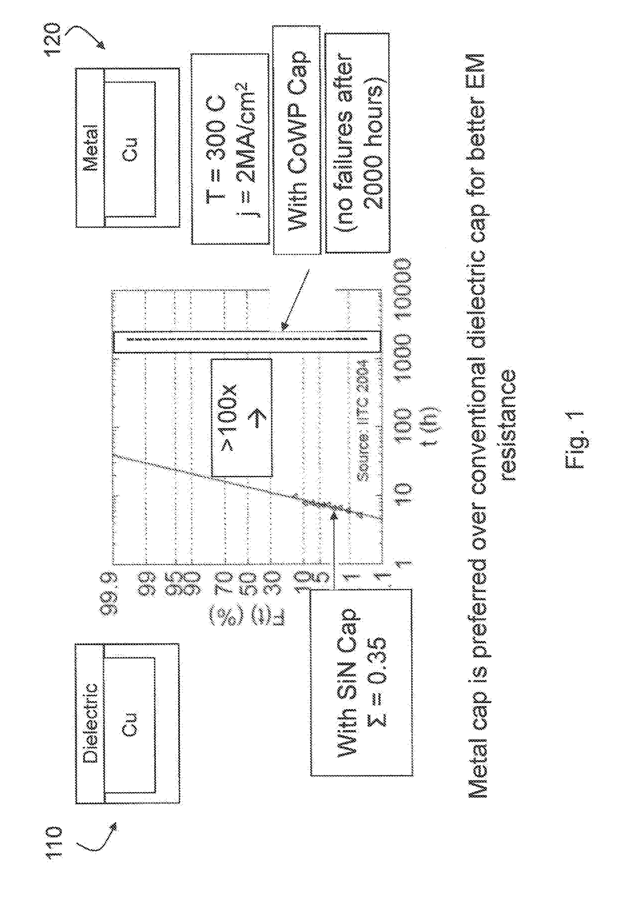
[0013]FIG. 1 schematically illustrates conventional caps for semiconductor structures to compare performance of metal caps and dielectric caps. Structure 110 shows a conventional cap formed of a dielectric layer. The structure includes semiconductor body having a cavity formed therein. The cavity is filled with a conductive material such as copper (Cu). While not shown, the structure may include a barrier (interchangeably, a liner) material interposed between the semiconductor body and the conductive material. Structure 120 illustrates a similar structure having a metal capping layer. Finally, FIG. 1 comparatively illustrates the advantage of having a metal capping layer over the dielectric layer for better EM resistance. In addition, the Cu / metal interface provides better adhesion strength than the Cu / dielectric interface, which results in better EM resistance in the Cu / metal capping layer system.

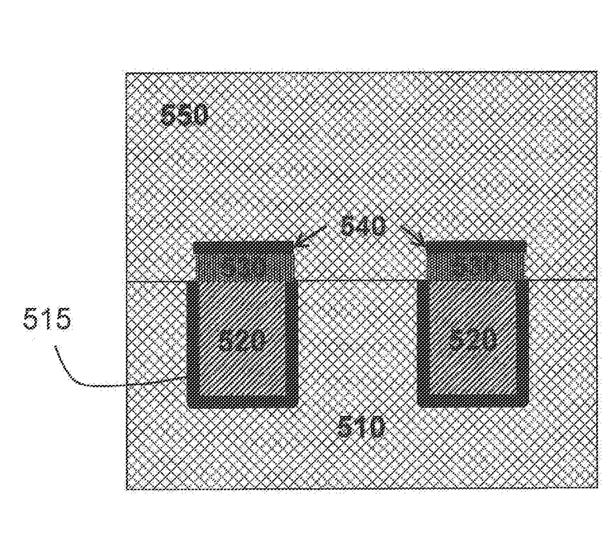
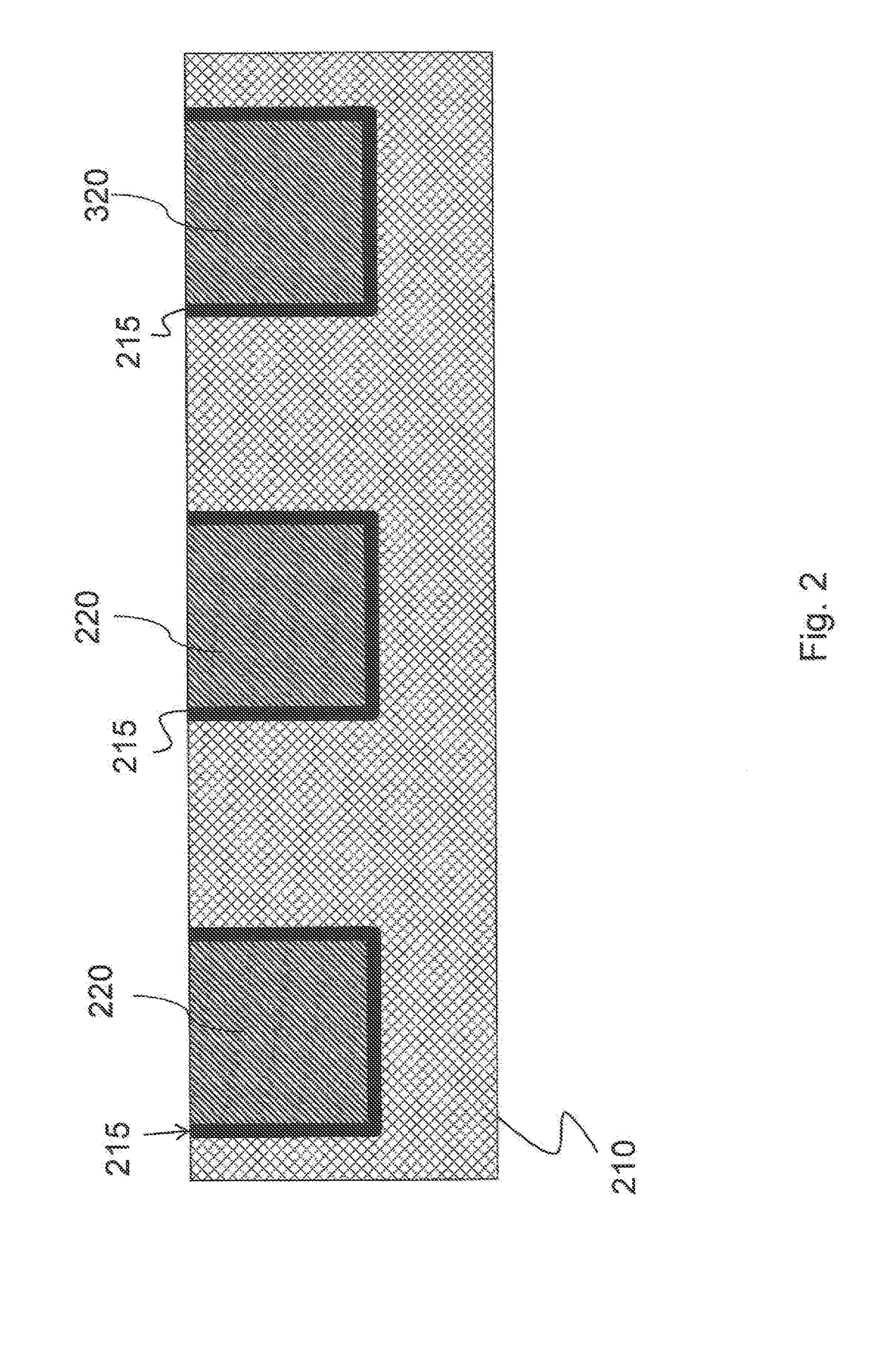
[0014]FIG. 2 illustrates semiconductor body 210 having three exemplary cavities formed...


PUM


Abstract

The disclosure relates to semiconductor interconnect structure having enhanced electromigration (EM) reliability in which an oxygen scavenger layer deposited (directly or indirectly) over a surface of conductive material. In one embodiment, the disclosure relates to semiconductor structure having a substrate having a cavity formed therein; a barrier material lining a portion of the cavity; a conductive material formed over the barrier material, the conductive material defining an interconnect layer; a metal cap formed over at least a portion of the conductive material; an oxygen scavenger layer formed over the metal cap layer, the oxygen scavenger layer comprising one or more of Al, TiAl or Al alloys, Mg, TiMg, Mg alloys, and deposited over the metal cap layer using one or more of a Chemical Vapor Deposition (CVD), Atomic Layer Deposition (ALD), Electroless Plating Deposition (ELD) electrodeless deposition techniques; wherein the oxygen scavenger layer removes oxygen from the interface between the conductive material surface and the metal cap layer.

Description

BACKGROUNDField[0001]The disclosure relates to a method, apparatus and structure for metal cap integration. Specifically, the disclosure relates to a semiconductor interconnect structure having enhanced electromigration (EM) reliability in which an oxygen scavenger layer deposited (directly or indirectly) over a surface of a conductive material. The conductive material may be embedded within a low dielectric constant k dielectric material.Description of Related Art[0002]Generally, semiconductor devices include a plurality of circuits which form an integrated circuit (IC) fabricated on a semiconductor substrate. A complex network of signal paths will normally be routed to connect the circuit elements distributed on the surface of the substrate. Efficient routing of these signals across the device requires formation of multilevel or multilayered schemes, such as, for example, single or dual damascene wiring structures. The wiring structure typically includes copper, Cu, since Cu based...

Claims


Application Information

Patent Timeline
IPC IPC(8): H01L23/522H01L23/532
CPCH01L23/53238H01L23/5226H01L23/53223
Inventor YANG, CHIH-CHAOEDELSTEIN, DANIEL CHARLES
Owner IBM CORP
Why Eureka
Try Eureka