

Perovskite light-emitting layer and manfuacturing method thereof, light-emitting device and display device
A perovskite and light-emitting layer technology, applied in the field of liquid crystal display, can solve the problems of low efficiency of tin-based perovskite light-emitting diodes
- Summary
- Abstract
- Description
- Claims
- Application Information
AI Technical Summary
Problems solved by technology
Method used
Image

Examples
no. 1 example
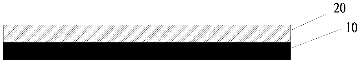
[0037] figure 1 It is a schematic diagram of the structure of the perovskite light-emitting layer according to the first embodiment of the present invention. Such as figure 1 As shown, a perovskite light-emitting layer includes a perovskite light-emitting film layer 10 and an encapsulation film layer 20 that wraps the perovskite light-emitting film layer 10, and the encapsulation film layer includes compound A. The formula is X 2+ SO 3 2- R, where X 2+ It is a divalent metal ion, and R is a benzene ring structure containing a hydroxyl functional group. Among them, R contains at least one benzene ring structure, for example, R can contain one benzene ring structure, two benzene ring structures connected together (naphthalene structure) or three benzene ring structures connected together (anthracene structure) . That is, the benzene ring structure R containing a hydroxyl functional group includes one or more of a benzene structure containing at least one hydroxyl functional grou...
no. 2 example
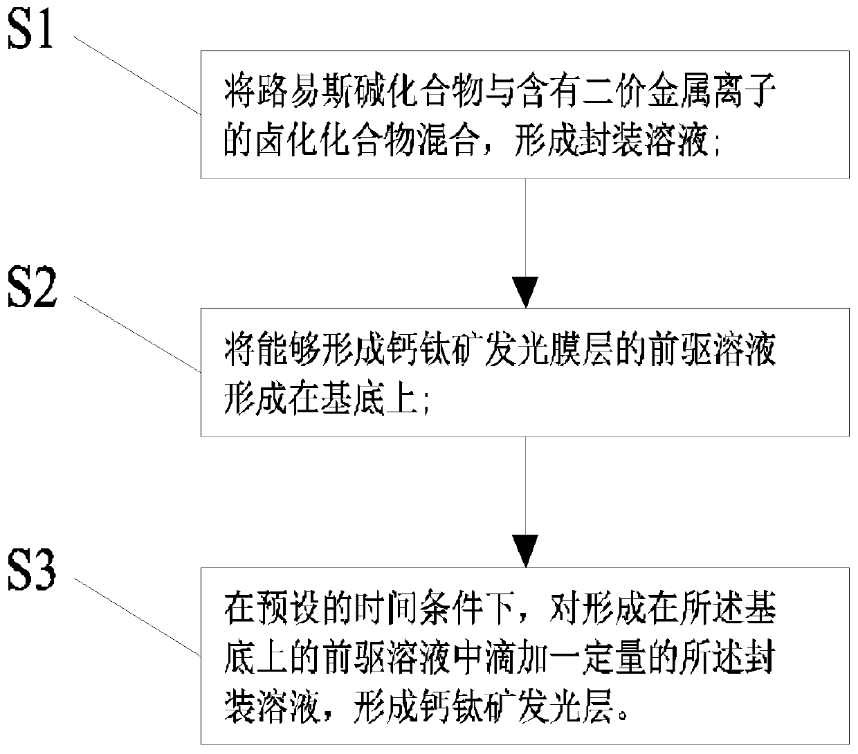
[0046] Based on the technical concept of the embodiment of the present invention, the embodiment of the present invention also provides a method for preparing the perovskite luminescent layer. figure 2 It is a flow chart of the preparation method of the perovskite luminescent layer in the second embodiment of the present invention. Such as figure 2 As shown, the preparation method of the perovskite luminescent layer includes:
[0047] S1. Mixing the Lewis base compound and the halogenated compound containing divalent metal ions to form an encapsulating solution;
[0048] S2, forming a precursor solution capable of forming a perovskite luminescent film layer on the substrate;
[0049] S3. Under a preset time condition, drop a certain amount of the packaging solution into the precursor solution formed on the substrate to form a perovskite light-emitting layer.
[0050] Among them, the halogenated compound can be one or more of fluorinated compounds, chlorinated compounds, brominated c...
no. 3 example
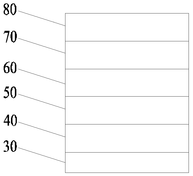
[0069] Figure 4 It is a schematic diagram of the structure of the light emitting diode in the third embodiment of the present invention. Figure 4 Shows the inverted structure of a tin-based perovskite light-emitting diode, such as Figure 4 As shown, the tin-based perovskite light-emitting diode includes a substrate 30, an electron transport layer 70, a perovskite light-emitting layer 60, a hole transport layer 50, a hole injection layer 40, and a cathode 80 which are sequentially stacked from bottom to top.
[0070] The manufacturing method of the above tin-based perovskite light-emitting diode includes:
[0071] (1) Pre-treat the substrate. The pretreatment of the substrate includes: ultrasonically cleaning the substrate with isopropanol and water, and then irradiating the substrate with ultraviolet for 5-10 minutes. Among them, the substrate is a conductive ITO glass substrate.
[0072] (2) Form an electron transport layer. The forming of the electron transport layer includ...
PUM
 Abstract
Description
Claims
Application Information