Supercharge Your Innovation With Domain-Expert AI Agents!

Method for producing an sgt-including semiconductor device

a technology of semiconductor devices and semiconductor chips, applied in semiconductor devices, digital storage, instruments, etc., can solve the problems of circuit chip cost reduction, and achieve the effect of high accuracy and high accuracy

Active Publication Date: 2017-10-19
UNISANTIS ELECTRONICS SINGAPORE PTE LTD
View PDF0 Cites 3 Cited by
  • Summary
  • Abstract
  • Description
  • Claims
  • Application Information

AI Technical Summary

Benefits of technology

The invention provides a method for producing a semiconductor device with a structure called an SGT (semiconductor-pillar-based structure), which has improved performance compared to previous methods. The method involves several steps, including forming a semiconductor pillar, creating impurity regions, adding a first insulating layer, forming a first gate insulating layer, adding a first gate conductor layer, etching the first insulating layer, adding a second insulating layer, etching the second insulating layer, adding a second gate conductor layer, and etching the first gate conductor layer. These steps are performed to create the SGT structure, which includes the semiconductor pillar, impurity regions, and a gate insulating layer. The method also includes steps to form a second insulating layer and a second gate conductor layer, as well as a third insulating layer and a third gate conductor layer. The technical effects of this method include improved performance of the SGT structure and simplified production process.

Problems solved by technology

Moreover, size reduction of circuit chips that use CMOS inverter circuits leads to cost reduction of circuit chips.

Method used


Image

  • Method for producing an sgt-including semiconductor device
  • Method for producing an sgt-including semiconductor device
  • Method for producing an sgt-including semiconductor device

Examples


first embodiment

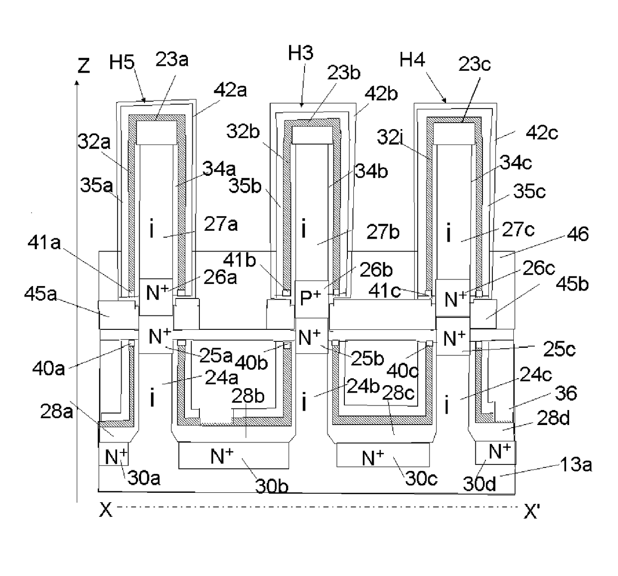
[0090]An SGT-including semiconductor device and a production method therefor according to a first embodiment are described below with reference to FIGS. 1A to 1C and 2AA to 2WC.

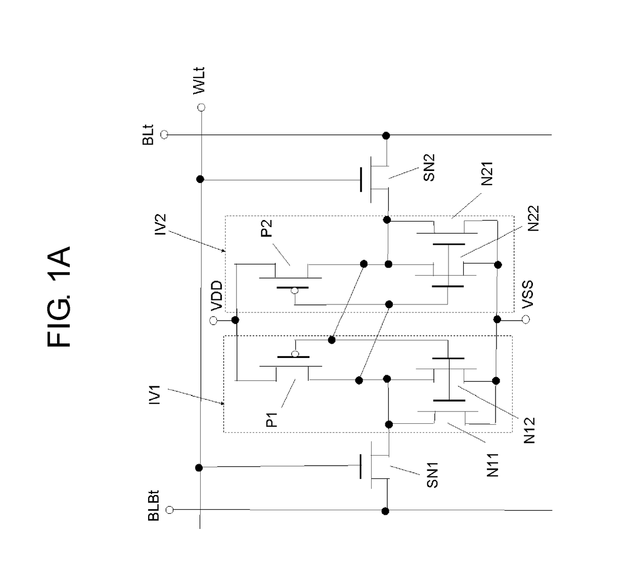
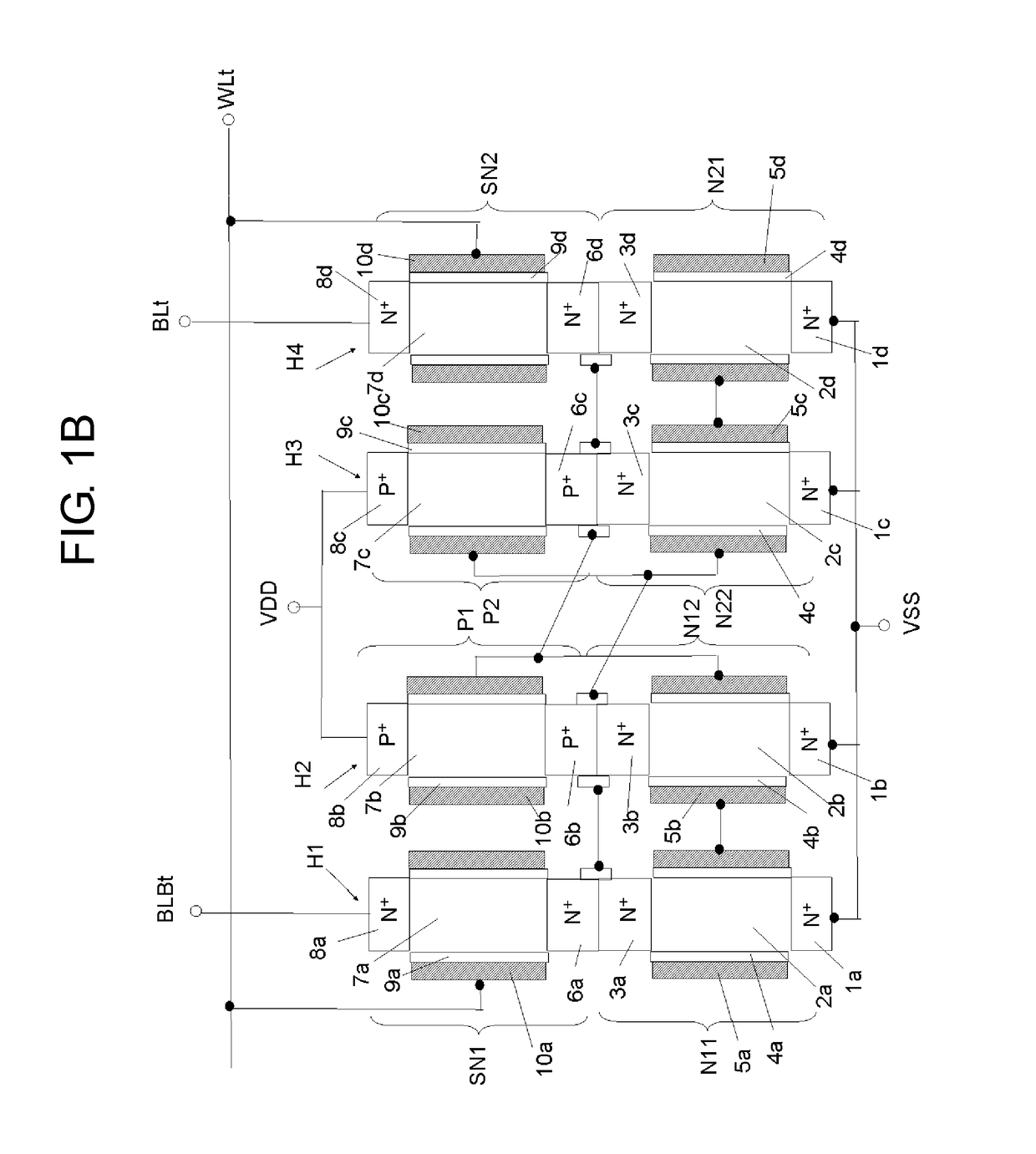
[0091]FIG. 1A is a circuit diagram of a static random access memory (SRAM) cell circuit according to this embodiment. The SRAM cell includes two inverter circuits IV1 and IV2. The inverter circuit IV1 is constituted by a P-channel SGT P1 serving as a load transistor and two N-channel SGTs N11 and N12 serving as drive transistors and being connected in parallel. The inverter circuit IV2 is constituted by a P-channel SGT P2 serving as a load transistor and two N-channel SGTs N21 and N22 serving as drive transistors and being connected in parallel. The gate of the P-channel SGT P1 of the inverter circuit IV1 is connected to the gates of the N-channel SGTs N11 and N12. The drain of the P-channel SGT P2 of the inverter circuit IV2 is connected to the drains of the N-channel SGTs N21 and N22. The gate of the P-chan...

second embodiment

[0139]A method for producing an SGT-including semiconductor device according to a second embodiment will now be described with reference to FIGS. 3AA to 3FC.

[0140]In the second embodiment, the same steps as those illustrated in FIGS. 2AA to 2JC are performed prior to a step shown in FIGS. 3AA to 3AC. The description therefor is thus omitted. Subsequent to the step shown in FIGS. 2JA to 2JC, resist layers 61a, 61b, 61c, and 61d are formed by applying a resist sensitive to light, an X-ray, or an electron beam and performing lithography, as shown in FIGS. 3AA to 3AC. The resist layer 61a is formed so as to surround the outer periphery of the Si pillar H5. The resist layer 61b is formed so as to come into contact with the Si-pillar-H4-side side wall of the Si pillar H3 and surround the outer periphery of the Si pillar H4. The resist layer 61c is formed so as to come into contact with the side wall of the Si pillar H2 and surround the outer periphery of the Si pillar H1. The resist layer...

third embodiment

[0148]A method for producing an SGT-including semiconductor device according to a third embodiment will now be described with reference to FIGS. 4AA to 4DC. In this embodiment, the technical idea of the present invention is applied to an SGT-CMOS inverter circuit. In FIGS. 4AA to 4DC, a drawing whose reference ends with A is a plan view, a drawing whose reference ends with B is a cross-sectional view taken along line X-X′, and a drawing whose reference ends with C is a cross-sectional view taken along line Y-Y′.

[0149]As illustrated in FIG. 4AA to 4AC, Si pillars H10a and H10b are formed on an i-layer substrate 66. A SiO2 layer 67 is formed around the Si pillars H10a and H10b and on the i-layer substrate 66. Gate insulating layers 68a and 68b are formed on the outer peripheries of the Si pillars H10a and H10b and gate conductor layers 69a and 69b composed of, for example, TiN are formed on the outer peripheries of the gate insulating layers 68a and 68b. A resist layer 70 is formed so...


PUM


Abstract

A method for producing an SGT-including semiconductor device includes forming a gate insulating layer on an outer periphery of a Si pillar, forming a gate conductor layer on the gate insulating layer, and forming an oxide layer on the gate conductor layer. Then a hydrogen fluoride ion diffusion layer containing hydrogen fluoride ions is formed so as to make contact with the oxide layer and lie at an intermediate position of the Si pillar. A part of the oxide film in contact with the hydrogen fluoride ion diffusion layer is etched and an opening is thereby formed on the outer periphery of the Si pillar.

Description

CROSS REFERENCES TO RELATED APPLICATIONS[0001]This application is a continuation-in-part of U.S. patent application Ser. No. 15 / 285,665, filed Oct. 5, 2016, which was a continuation of U.S. patent application Ser. No. 14 / 732,208, filed Jun. 5, 2015, now U.S. Pat. No. 9,514,944 B2, which was a continuation of international patent application PCT / JP2013 / 063701, filed May 16, 2013. The contents of all these applications are incorporated herein by reference in their entirety.BACKGROUND OF THE INVENTIONField of the Invention[0002]The present invention relates to a method for producing a semiconductor device that includes surrounding gate MOS transistors (SGTs).Description of the Related Art[0003]Applications of surrounding gate MOS transistors (hereinafter referred to as SGTs) to semiconductor elements that offer highly integrated semiconductor devices have expanded in recent years and higher integration of SGT-including semiconductor devices is pursued under such trends.[0004]FIG. 6 sho...

Claims


Application Information

Patent Timeline
Patent Type & Authority Applications(United States)
IPC IPC(8): H01L27/11H01L29/78H01L29/66H01L29/423H01L21/311H01L21/28H01L29/786H10B10/00G11C11/412
CPCH01L27/1108G11C11/412H01L29/42392H01L29/7827H01L21/28158H01L29/66666H01L29/42356H01L21/31116H01L21/28247H01L29/78642H10B10/125
Inventor MASUOKA, FUJIOHARADA, NOZOMU
Owner UNISANTIS ELECTRONICS SINGAPORE PTE LTD
Features
  • R&D
  • Intellectual Property
  • Life Sciences
  • Materials
  • Tech Scout
  • Unparalleled Data Quality
  • Higher Quality Content
  • 60% Fewer Hallucinations
Learn More