Compound for organic electric element, organic electric element comprising the same and electronic device thereof

a technology of organic electric elements and organic electric elements, which is applied in the direction of luminescent compositions, organic chemistry, chemistry apparatus and processes, etc., can solve the problems of power consumption, efficiency and life span, and power consumption is an important issue, so as to improve the luminous efficiency, color purity and life span of the device, and the effect of lowering the driving voltage of organic electronic elements

Active Publication Date: 2017-10-19
DUK SAN NEOLUX
View PDF1 Cites 9 Cited by
  • Summary
  • Abstract
  • Description
  • Claims
  • Application Information

AI Technical Summary

Benefits of technology

[0013]In order to solve one or more of the above-mentioned problems occurring in the prior art, an aspect of the present invention is to provide a compound capable of lowering the driving voltage of an organic electronic element and improving the luminous efficiency, color purity and life span of the device, an organic electric element employing such a compound, and an electronic device thereof.

Problems solved by technology

Currently, the power consumption is required more and more as size of display becomes larger and larger in the portable display market.
Therefore, the power consumption is an important factor in the portable display with a limited power source of the battery, and efficiency and life span issue also must be solved.
However, efficiency cannot be maximized only by simply improving the organic material layer.
As a result, a charge unbalance occurs in the light emitting layer, and light emission occurs in the hole transport layer or at the interface of the hole transport layer, resulting in showing poor color purity, reduced efficiency, and low life span.
In addition, when a material having a high hole mobility is used to make a low driving voltage, the efficiency tends to decrease.
This is because the hole mobility is faster than the electron mobility in a general organic electronic element, resulting in a charge unbalance in the light emitting layer.
As a result, efficiency and life span are decreased.
However, this cannot be achieved simply by the structural properties of the core of an emission-auxiliary layer material, but is possible when the combination of the core and sub-substituent properties of the material is combined.
However, such a stable and efficient organic material layer material for an organic electric element has not yet been fully developed.
Meanwhile, even when a similar core is used, it is very difficult to infer the characteristics of an emission-auxiliary layer if a used organic material layer varies, because the correlation between the emission-auxiliary layer and a hole transport layer and between the emission-auxiliary layer and a light emitting layer (host) must be figured out.

Method used


Image

  • Compound for organic electric element, organic electric element comprising the same and electronic device thereof
  • Compound for organic electric element, organic electric element comprising the same and electronic device thereof
  • Compound for organic electric element, organic electric element comprising the same and electronic device thereof

Examples


example 28

[Example 2] to [Example 28]

Green OLED (An Emission-Auxiliary Layer)

[0130]The OLEDs were fabricated in the same manner as described in Example 1 except that any one of the inventive compounds described in Table 4 instead of the inventive compound 1-1 was used as an emission-auxiliary layer material.

example 29

Red OLED (An Emission-Auxiliary Layer)

[0134]Organic light emitting diodes (OLEDs) were fabricated according to a conventional method by using a compound of the present invention as an emission-auxiliary layer material.

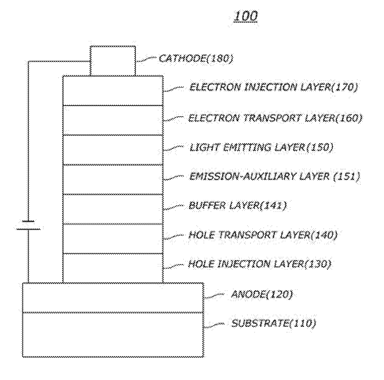
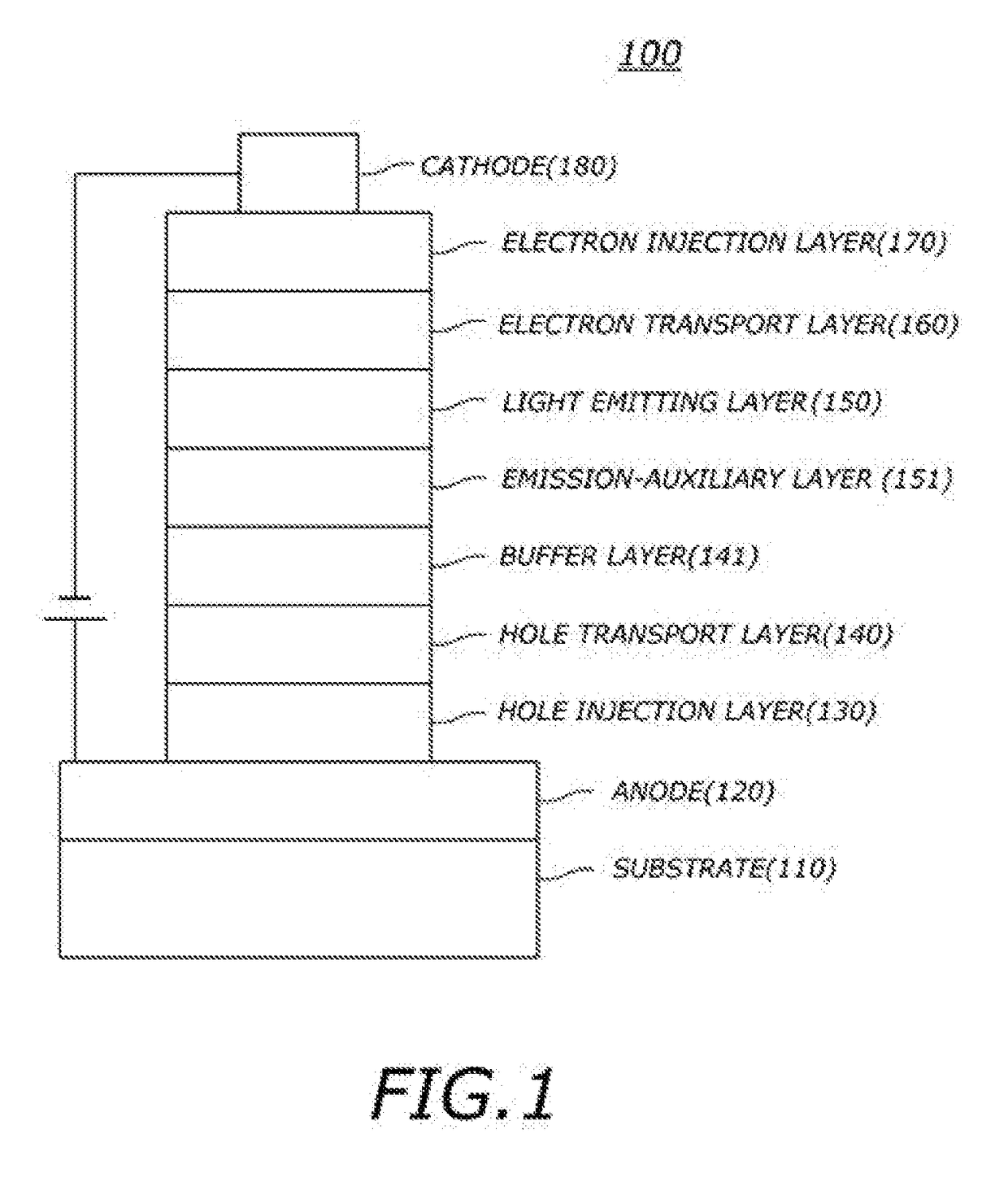
[0135]First, an ITO layer (anode) was formed on a glass substrate, and a film of 2-TNATA was vacuum-deposited on the ITO layer to form a hole injection layer with a thickness of 60 nm. Subsequently, NPB was vacuum-deposited with a thickness of 60 nm on the hole injection layer to form a hole transport layer.

[0136]Subsequently, the compound 1-2 of the present invention was vacuum-deposited on the hole transport layer to form a emission-auxiliary layer with a thickness of 20 nm.

[0137]A light emitting layer with a thickness of 30 nm was deposited on the emission-auxiliary layer by using the CBP as a host material and bis-(1-phenylisoquinolyl)iridium(III)acetylacetonate (“(piq)2Ir(acac)”) as a dopant material in a weight ratio of 95:5.

[0138]Next, BAlq was vacuum-deposited ...

example 30

[Example 30] to [Example 56]

Red OLED (An Emission-Auxiliary Layer)

[0140]The OLEDs were fabricated in the same manner as described in Example 29 except that any one of the inventive compounds described in Table 5 instead of the inventive compound 1-2 was used as an emission-auxiliary layer material.


PUM

PropertyMeasurementUnit
thicknessaaaaaaaaaa
thicknessaaaaaaaaaa
thicknessaaaaaaaaaa

Abstract

Provided are a compound of Formula 1 and an organic electric element comprising a first electrode, a second electrode, and an organic material layer formed between the first electrode and the second electrode, and electronic device comprising the organic electric element, wherein the luminous efficiency and life span can be improved and the driving voltage of the organic electronic device can be lowered by comprising the compound represented by Formula 1 in the organic material layer.

Description

CROSS-REFERENCE TO RELATED APPLICATION[0001]This patent application claims benefit under 119(a) (35 U.S.C. §119(a)) to Korean Patent Application No. 10-2014-0133993, filed on Oct. 6, 2014, the contents of which are hereby incorporated by reference for all purposes as if fully set forth herein.BACKGROUNDTechnical Field[0002]The present invention relates to compounds for organic electric elements, organic electric elements comprising the same, and electronic devices thereof.Background Art[0003]In general, an organic light emitting phenomenon refers to a phenomenon in which electric energy is converted into light energy of an organic material. An organic electric element utilizing the organic light emitting phenomenon usually has a structure including an anode, a cathode, and an organic material layer interposed therebetween. In many cases, the organic material layer may have a multilayered structure including multiple layers made of different materials in order to improve the efficien...

Claims


Application Information

Patent Timeline
Patent Type & Authority Applications(United States)
IPC IPC(8): H01L51/00H01L51/50C07D209/82
CPCH01L51/0072H01L51/5092C07D209/82H01L51/0096C07D209/88C09K11/06C09K2211/1029H10K85/6572C07D409/14Y02E10/549H10K85/654H10K85/633H10K85/6576H10K50/15H10K50/11H10K50/171H10K77/10
Inventor LEE, BUMSUNG
Owner DUK SAN NEOLUX
Why Eureka
Try Eureka