Antireflection film, and optical member and optical apparatus each using the antireflection film

a technology of antireflection film and optical member, applied in the direction of instruments, coatings, optics, etc., can solve the problems of reducing production cost, requiring extremely large-scale equipment etc., and achieves effective antireflection effect, poor broadband reflectance characteristic of antireflection film, and restricted production cost

Active Publication Date: 2017-11-02
CANON KK
View PDF3 Cites 6 Cited by
  • Summary
  • Abstract
  • Description
  • Claims
  • Application Information

AI Technical Summary

Benefits of technology

[0010]However, the content disclosed in Japanese Patent Application Laid-Open No. S61-51283 has a problem in that the broadband reflectance characteristic of the antireflection film is poor. In addition, the antireflection effect of such antireflection film significantly depends on its thickness. When an actual thickness deviates from a design thickness, an effective antireflection effect is not obtained. Accordingly, there is a problem in that high-precision thickness control is required, and hence the reduction of production cost is restricted.

Problems solved by technology

S61-51283 has a problem in that the broadband reflectance characteristic of the antireflection film is poor.
Accordingly, there is a problem in that high-precision thickness control is required, and hence the reduction of production cost is restricted.
In addition, in the case of the method involving forming a fine pattern with a fine processing apparatus as disclosed in Japanese Patent Application Laid-Open No. 2012-118501, such pattern forming method generally requires extremely large-scale equipment, and hence requires an extremely expensive equipment investment.
Further, although the method is suitable for the formation of the pattern on a flat surface, the method has a problem in that it is extremely difficult to form the pattern on a complicated shape, for example, a curved surface.
The method is not suitable for application to a general-purpose optical element, such as a lens.
Consequently, the growth of the protrusions stops, and the height of the structural body cannot be increased.
Accordingly, there is a problem in that the fine structural body cannot be formed to have a height needed for the prevention of reflection in a broad band.
Therefore, even when a layer is formed under the fine structural body so that the refractive index may smoothly change, the thickness of the layer in which the refractive index smoothly changes cannot be increased owing to the remaining alumina layer.
Accordingly, there is a problem in that a broadband antireflection structural body cannot be formed.

Method used


Image

  • Antireflection film, and optical member and optical apparatus each using the antireflection film
  • Antireflection film, and optical member and optical apparatus each using the antireflection film
  • Antireflection film, and optical member and optical apparatus each using the antireflection film

Examples


example 1

[0073]In Example 1, an optical member including the antireflection film of the present invention was produced and evaluated by the following methods.

[0074](Aluminum Oxide Precursor Sol)

[0075]14.8 g of aluminum-sec-butoxide (ASBD, manufactured by Kawaken Fine Chemicals Co., Ltd.), 3-methyl-2,4-pentanedione serving as a stabilizer in an amount of 0.5 molar equivalent to the aluminum-sec-butoxide, and 2-ethylbutanol were mixed and stirred to uniformity. 0.01 M dilute hydrochloric acid was dissolved in a 2-ethylbutanol / 1-ethoxy-2-propanol mixed solvent, and then the solution was slowly added to the solution of the aluminum-sec-butoxide. The mixture was stirred for a while. The solvent was adjusted so as to finally be 59.3 g of a mixed solvent having a mixing ratio of 2-ethylbutanol and 1-ethoxy-2-propanol of 7 / 3. Further, the resultant was stirred in an oil bath at 120° C. for 2 hours to prepare an aluminum oxide precursor sol.

[0076](Hollow Particle-Dispersed Coating Material)

[0077]As a...

example 2

[0091]In Example 2, two kinds of optical members including antireflection films including particle layers having different thicknesses were produced.

[0092]After a substrate had been coated with an amorphous aluminum oxide film in the same manner as in Example 1, an application liquid of hollow particles was formed into a film by a spin coating method for 60 seconds at each of 2,000 rpm and 4,000 rpm. As a result, substrates having particle layers made of hollow particles having thicknesses of 142 nm and 105 nm formed on the amorphous aluminum oxide film were obtained. Each of the substrates was immersed in warm water at 75° C. for 20 minutes to provide an optical member of this Example.

[0093](Evaluation)

[0094]As in Example 1, the measurement results of reflectance are shown in FIG. 5. The optical member in which the particle layer formed at 2,000 rpm had a thickness of 142 nm was able to serve as an optical member satisfactory in an infrared region as compared to Example 1. In addit...

example 3

[0095](Film Formation)

[0096]In this Example, an optical member was obtained in the same manner as in Example 1 except that S-LAH55V (manufactured by Ohara Inc.) was used as a substrate.

[0097](Evaluation)

[0098]As in Example 1, the measurement result of the reflectance of the optical member of Example 3, and the reflectance of the S-LAH55V substrate used in Example 3 are shown in FIG. 6. The optical member of Example 3 was able to achieve a satisfactory reflectance over a visible to infrared region.


PUM

PropertyMeasurementUnit
thicknessaaaaaaaaaa
thicknessaaaaaaaaaa
particle diameteraaaaaaaaaa

Abstract

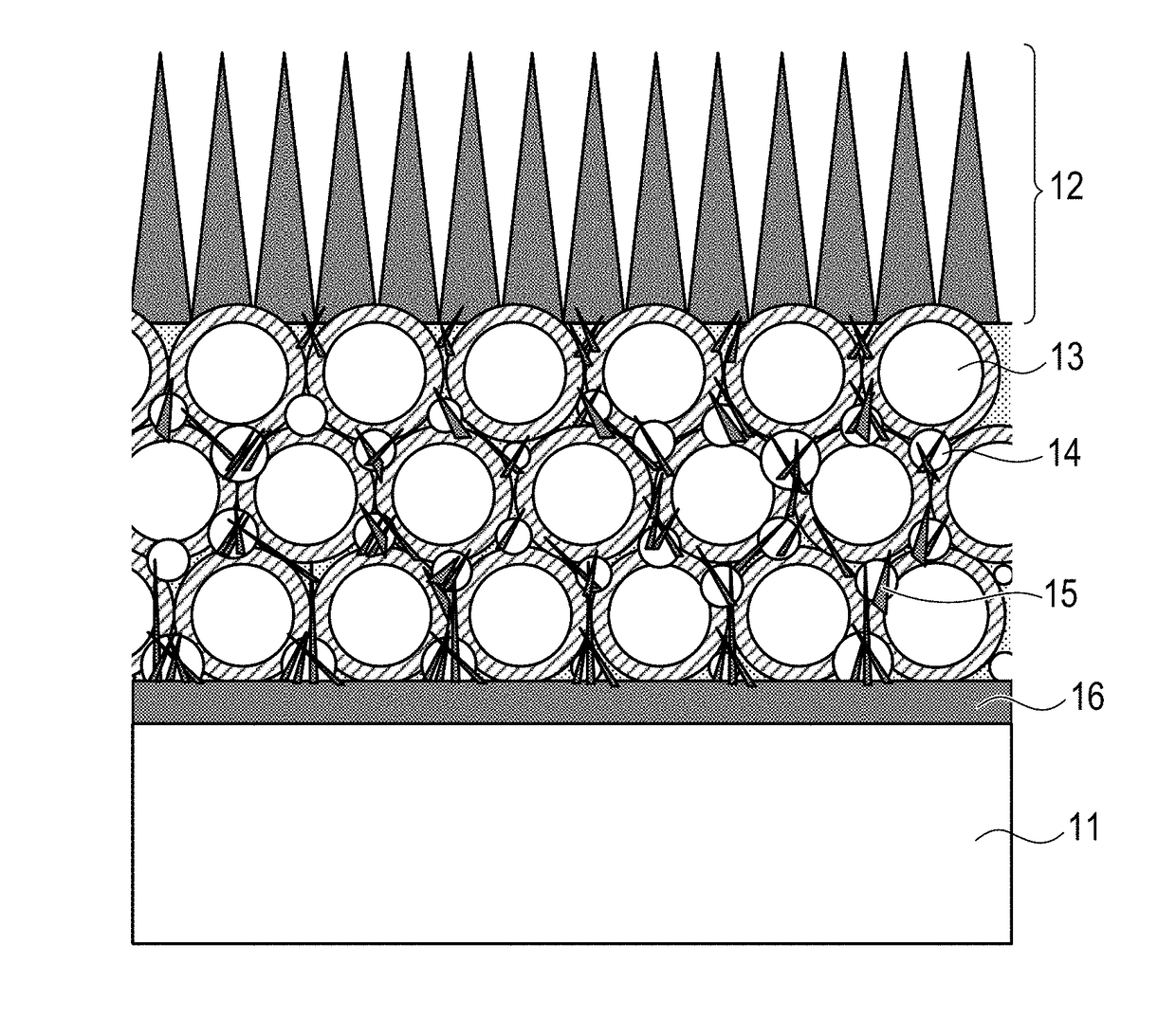
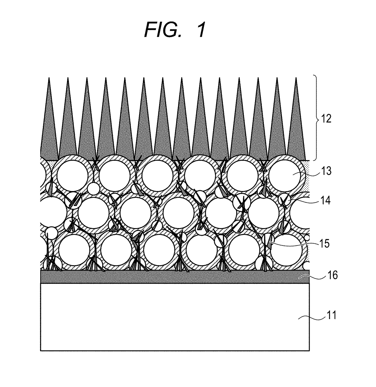
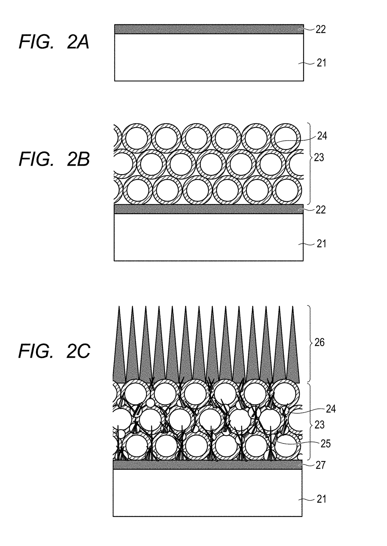
Provided are an antireflection film having a high antireflection effect in a broad band, including, on a substrate, in this order: a particle layer containing particles; and a layer having a textured structure containing aluminum oxide as a main component, in which the particle layer has an aluminum oxide textured structure between the particles, and an optical member and an optical apparatus each using the antireflection film.

Description

BACKGROUND OF THE INVENTIONField of the Invention[0001]The present invention relates to an antireflection film having a high antireflection effect in a broad band, and an optical member and an optical apparatus each using the antireflection film.Description of the Related Art[0002]An optical element, for example, a lens, to be included in an optical system is produced using a transparent material, for example, optical glass or an optical plastic. Such transparent material has a high refractive index, and hence has a high reflectance. When the reflectance is high, an effective amount of light that reaches an image surface is decreased, and moreover, a ghost or a flare occurs owing to unnecessary reflection. Accordingly, the optical element formed of the transparent material needs to have an antireflection function imparted thereto.[0003]As a technique for imparting the antireflection function to the optical element, there is generally known a multilayer antireflection film in which a...

Claims


Application Information

Patent Timeline
Patent Type & Authority Applications(United States)
IPC IPC(8): G02B1/115G02B27/00G02B1/118C03C17/25C03C17/00
CPCG02B1/115G02B1/118C03C17/25C03C17/007G02B27/0018C03C2217/478C03C2218/116C03C2217/73C03C2218/113C03C2218/31C03C2217/465G02B2207/109C03C17/34
Inventor OGANE, MASANOBU
Owner CANON KK
Why Eureka
Try Eureka