Light-emitting diode device for enhancing light extraction efficiency and current injection efficiency

a technology of light-emitting diodes and diodes, which is applied in the direction of semiconductor devices, basic electric elements, electrical equipment, etc., can solve the problems of reducing light extraction efficiency, o/m/o structure may have a significantly low sheet resistance, and not being free from light absorption issues, etc., and achieves high light extraction efficiency

Active Publication Date: 2017-12-14
KOREA UNIV RES & BUSINESS FOUND
View PDF1 Cites 9 Cited by
  • Summary
  • Abstract
  • Description
  • Claims
  • Application Information

AI Technical Summary

Benefits of technology

[0012]Some embodiments of the inventive concept provide a lateral or vertical LED device, in which an n or p electrode is replaced with a metal oxide / metal / metal oxide (O / M / O) structure allowing for high light extraction efficiency.

Problems solved by technology

The upper electrode may be formed of at least one of opaque metallic materials (e.g., Cr, Al, Ni, or Au), thereby reducing light extraction efficiency.
In addition, the O / M / O structure may have a significantly low sheet resistance, compared to a typical transparent electrode (e.g., ITO) of the same thickness.
However, if the electrode is formed of a metallic material, it is not free from a light absorption issue.
Since such materials are opaque, the electrode may prevent light from being emitted therethrough and may lead to deterioration in light extraction efficiency of an LED device.
In addition, the O / M / O structure may have a significantly low sheet resistance, compared to a transparent electrode (e.g., ITO) of the same thickness.

Method used


Image

  • Light-emitting diode device for enhancing light extraction efficiency and current injection efficiency
  • Light-emitting diode device for enhancing light extraction efficiency and current injection efficiency
  • Light-emitting diode device for enhancing light extraction efficiency and current injection efficiency

Examples


Embodiment Construction

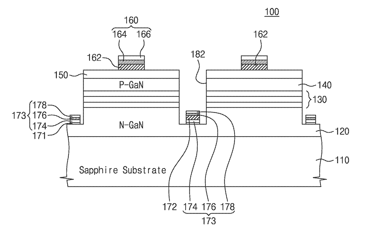
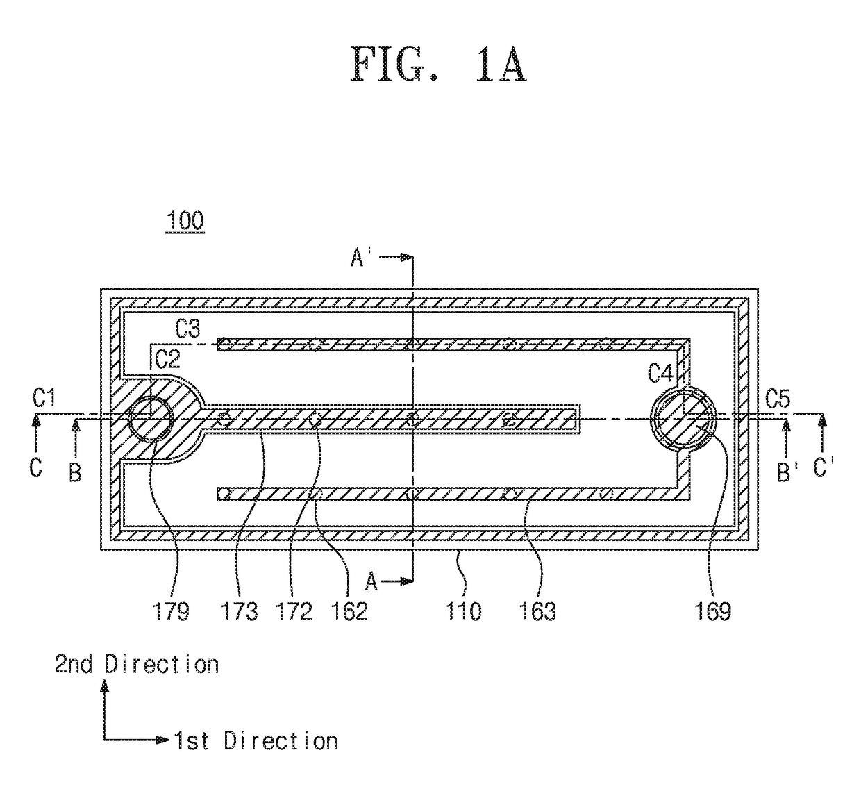
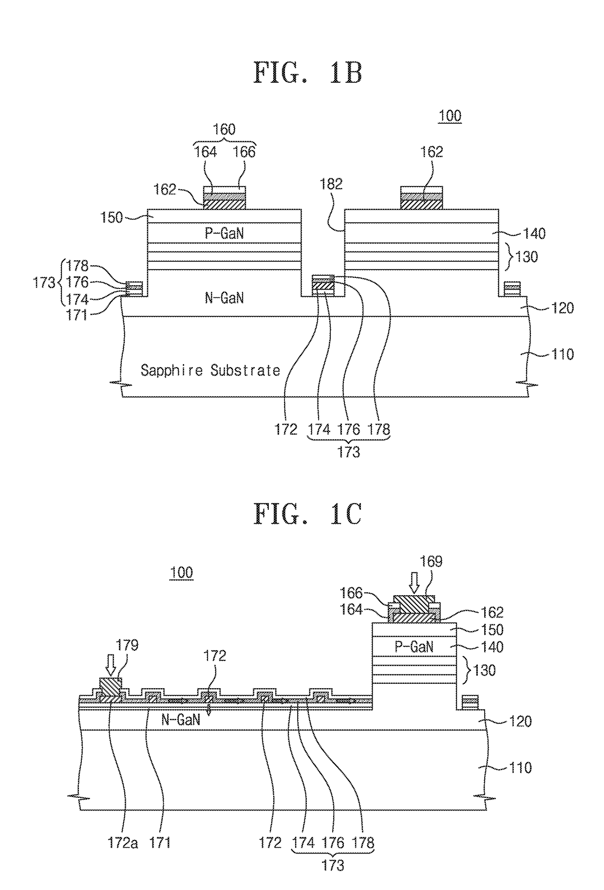
[0043]In a metal oxide / metal / metal oxide (O / M / O) structure, a material with high refractive index (e.g., ITO, TiO2, SnO2, ZnO, AZO, or Y2O3) is used as the metal oxide layer, and a material (e.g., silver (Ag) or silver alloys) having a low absorption coefficient for visible light is used as the metal layer. By controlling a thickness of each of the metal oxide layer and the metal layer, it may be possible to realize high transmittance within a specific wavelength range (e.g., red, green, or blue).

[0044]In the lateral LED, a transparent conductive metal oxide layer of the O / M / O structure may be used as a part of a current spreading layer that is directly provided under a p electrode. In some embodiments, ITO, SnO2, or ZnO may be used as the transparent conductive metal oxide material. Thus, in the case where the O / M / O structure is used to replace the p electrode, a transparent conductive metal oxide layer, which is positioned at the lowermost level in the O / M / O structure, may be used...


PUM


Abstract

Provided is a GaN light-emitting diode (LED) device. The LED device may include a substrate, an n-type GaN layer on the substrate, an active layer on the n-type GaN layer, a p-type GaN layer on the active layer, a current spreading layer including a transparent conductive metal oxide material on the p-type GaN layer, a plurality of upper current injection electrodes provided on the current spreading layer to be spaced apart from each other, an upper electrode pattern extending to cover the upper current injection electrodes, and an upper electrode pad electrically connected to the upper electrode pattern. The upper electrode pattern may include first and second upper electrode patterns, which are sequentially stacked and are a silver or silver alloy thin layer and a transparent conductive metal oxide thin layer, respectively.

Description

CROSS-REFERENCE TO RELATED APPLICATIONS[0001]This U.S. non-provisional patent application claims priority under 35 U.S.C. §119 to Korean Patent Application No. 10-2016-0071679, filed on Jun. 9, 2016, in the Korean Intellectual Property Office, the entire contents of which are hereby incorporated by reference.BACKGROUND OF THE INVENTION[0002]The present disclosure relates to a light-emitting diode (LED) device, and in particular, to an LED device, which has a structure of transparent metal oxide / metal / transparent metal oxide for enhancing light extraction efficiency and current injection efficiency, and which is provided with current injection electrodes for increasing current injection efficiency.[0003]Electron-hole recombination may occur at a junction region of p- and n-type semiconductor materials, when an electric current is provided to the junction region. A light emitting diode (LED) is a semiconductor device that is configured to generate light using such electron-hole recomb...

Claims


Application Information

Patent Timeline
Patent Type & Authority Applications(United States)
IPC IPC(8): H01L33/42H01L33/14H01L33/32H01L33/06
CPCH01L33/42H01L33/32H01L33/145H01L33/06H01L33/20H01L33/38H01L33/0008H01L33/02H01L33/14H01L2924/12041
Inventor SEONG, TAE YEONLEE, JEE-YUNKIM, DAE-HYUNKIM, KI SEOK
Owner KOREA UNIV RES & BUSINESS FOUND
Why Eureka
Try Eureka