Illumination System for a Lithographic or Inspection Apparatus

a technology of lithographic or inspection apparatus and illumination system, which is applied in the direction of lighting and heating apparatus, photomechanical apparatus, instruments, etc., can solve the problems of unreliability, reduced light availability, and high cost of conventional illumination system that provides different wavelengths and/or flexible illumination profiles

Inactive Publication Date: 2018-01-04
ASML NETHERLANDS BV
View PDF3 Cites 3 Cited by
  • Summary
  • Abstract
  • Description
  • Claims
  • Application Information

AI Technical Summary

Benefits of technology

The patent describes an illumination source that can produce light of different wavelengths and has a flexible pupil profile. This source is suitable for use in lithographic or inspection apparatus. The technical effect is a more efficient and flexible tool for adjusting the wavelength of light in these applications.

Problems solved by technology

This ultimately puts a practical limit on the number of modes available.
However, both aperture plates and SLMs reduce the amount of light available by ultimately blocking a portion of the light from the source.
Conventional illumination systems that provide different wavelengths and / or flexible illumination profiles are expensive, are not compact and are complex, and therefore unreliable.

Method used


Image

  • Illumination System for a Lithographic or Inspection Apparatus
  • Illumination System for a Lithographic or Inspection Apparatus
  • Illumination System for a Lithographic or Inspection Apparatus

Examples


Embodiment Construction

[0033]Before describing embodiments of the invention in detail, it is instructive to present an example environment in which embodiments of the present invention may be implemented.

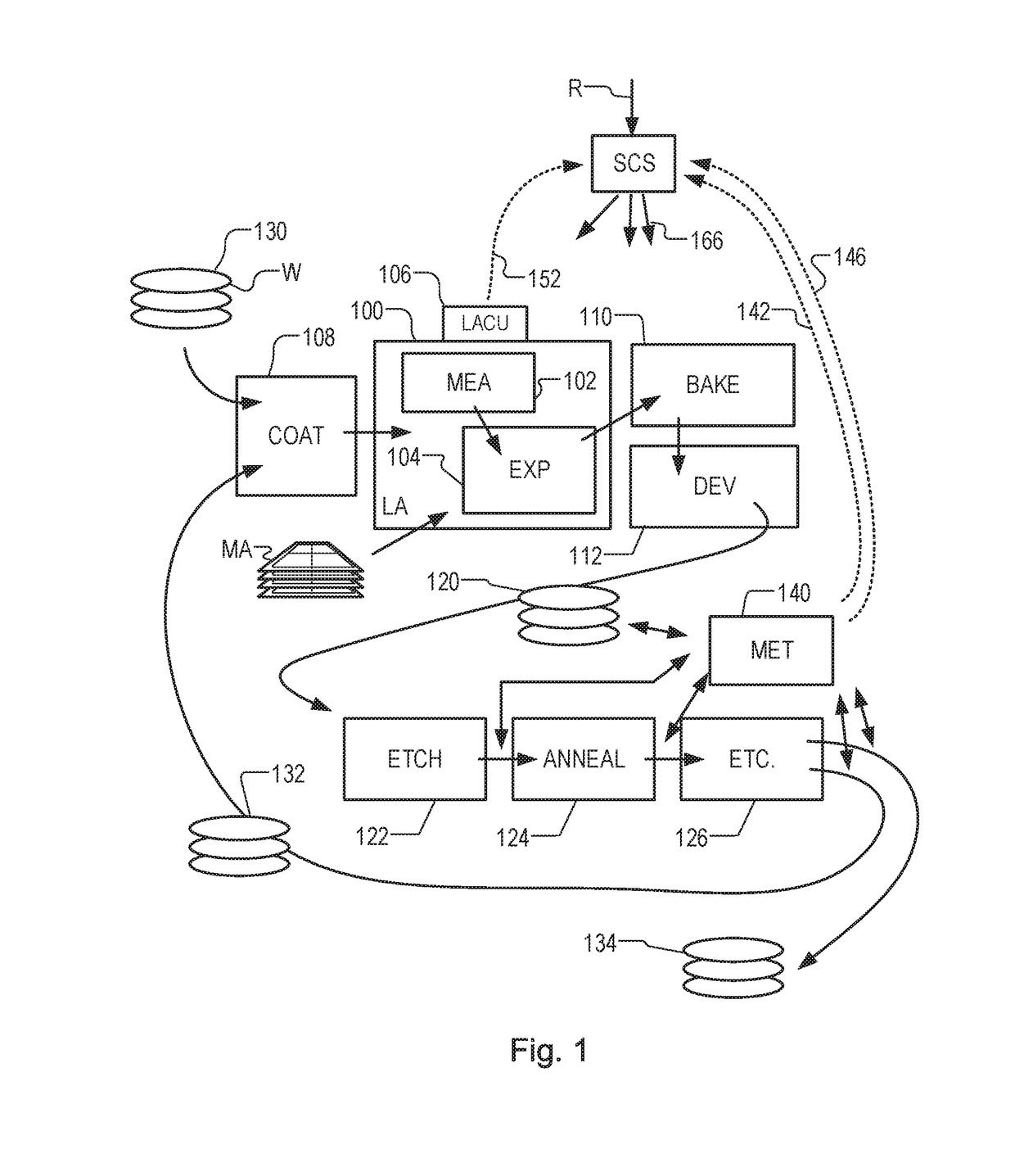
[0034]FIG. 1 at 100 shows a lithographic apparatus LA as part of an industrial facility implementing a high-volume, lithographic manufacturing process. In the present example, the manufacturing process is adapted for the manufacture of for semiconductor products (integrated circuits) on substrates such as semiconductor wafers. The skilled person will appreciate that a wide variety of products can be manufactured by processing different types of substrates in variants of this process. The production of semiconductor products is used purely as an example which has great commercial significance today.

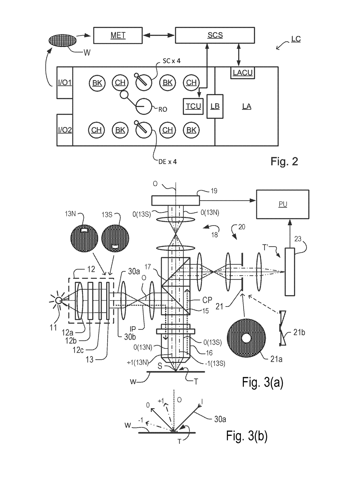
[0035]Within the lithographic apparatus (or “litho tool”100 for short), a measurement station MEA is shown at 102 and an exposure station EXP is shown at 104. A control unit LACU is shown at 106. In this example...


PUM


Abstract

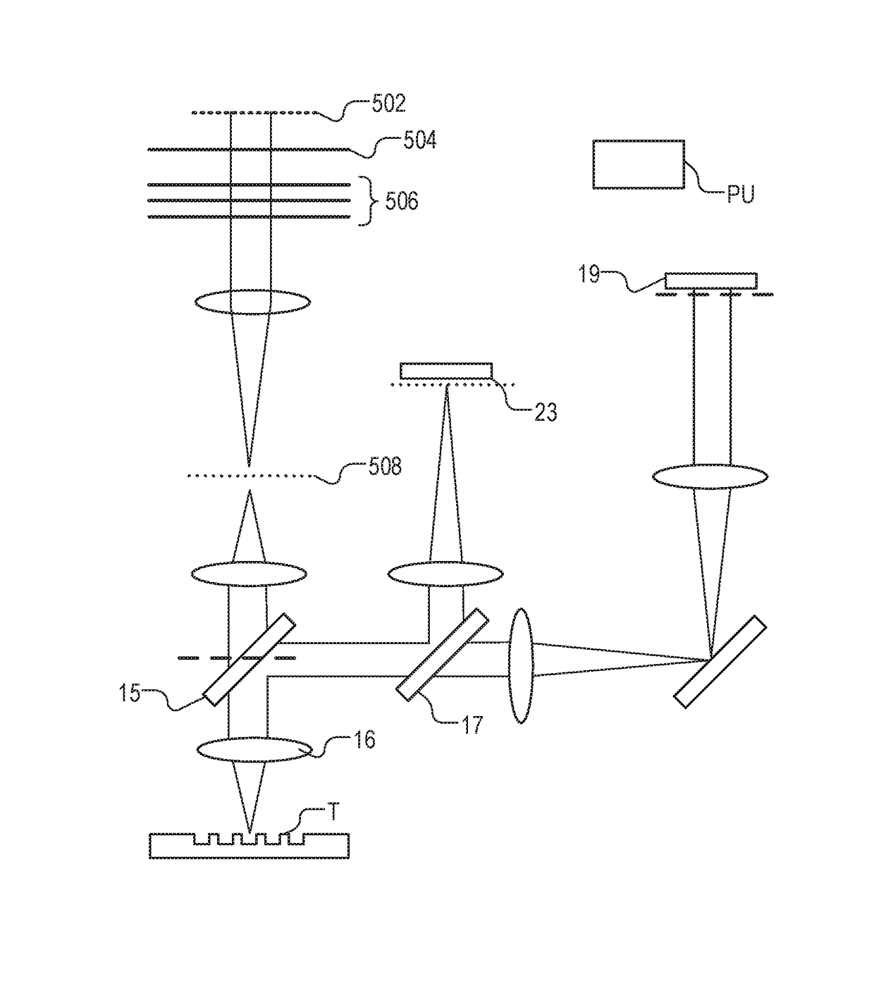
An illumination system has a microLED array 502. The microLED array 502 is imaged or placed very close to a phosphor coated glass disc 504 which upconverts the light from the microLED array into a narrow band emission. The plate has at least two different photoluminescent materials arranged to be illuminated by the microLED array and to thereby emit output light. The different photoluminescent materials have different emission spectral properties of the output light, e.g. different center wavelength and optionally different bandwidth. Illumination of different photoluminescent materials by the illumination sources is selectable, by selective activation of the microLEDs or by movement of the photoluminescent materials relative to the illumination sources, to provide different illumination of the different photoluminescent materials. This provides tunable spectral properties of the output light. Selectively configurable filters 506 are arranged to filter the output light in accordance with the selected illumination of the different photoluminescent materials.

Description

BACKGROUNDField of the Invention[0001]The present invention relates to an illumination system for a lithographic or inspection apparatus usable, for example, in the manufacture of devices by lithographic techniques.Background Art[0002]A lithographic apparatus is a machine that applies a desired pattern onto a substrate, usually onto a target portion of the substrate. A lithographic apparatus can be used, for example, in the manufacture of integrated circuits (ICs). In that instance, a patterning device, which is alternatively referred to as a mask or a reticle, may be used to generate a circuit pattern to be formed on an individual layer of the IC. This pattern can be transferred onto a target portion (e.g., including part of, one, or several dies) on a substrate (e.g., a silicon wafer). Transfer of the pattern is typically via imaging onto a layer of radiation-sensitive material (resist) provided on the substrate. In general, a single substrate will contain a network of adjacent ta...

Claims


Application Information

Patent Timeline
IPC IPC(8): G03F7/20F21V9/16F21V14/08
CPCG03F7/70191F21V9/16F21Y2115/10G03F7/7005F21V14/08G03F7/70575G03F7/70625G03F7/70633F21V9/30
Inventor TUKKER, TEUNIS WILLEMPANDEY, NITESHVERSCHUREN, COEN ADRIANUS
Owner ASML NETHERLANDS BV
Why Eureka
Try Eureka