Lead frame and method of fabricating the same
- Summary
- Abstract
- Description
- Claims
- Application Information
AI Technical Summary
Benefits of technology
Problems solved by technology
Method used
Image
Examples
embodiment
Fundamental Embodiment
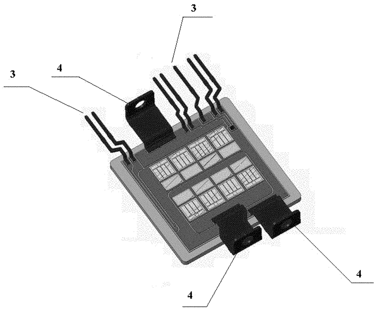
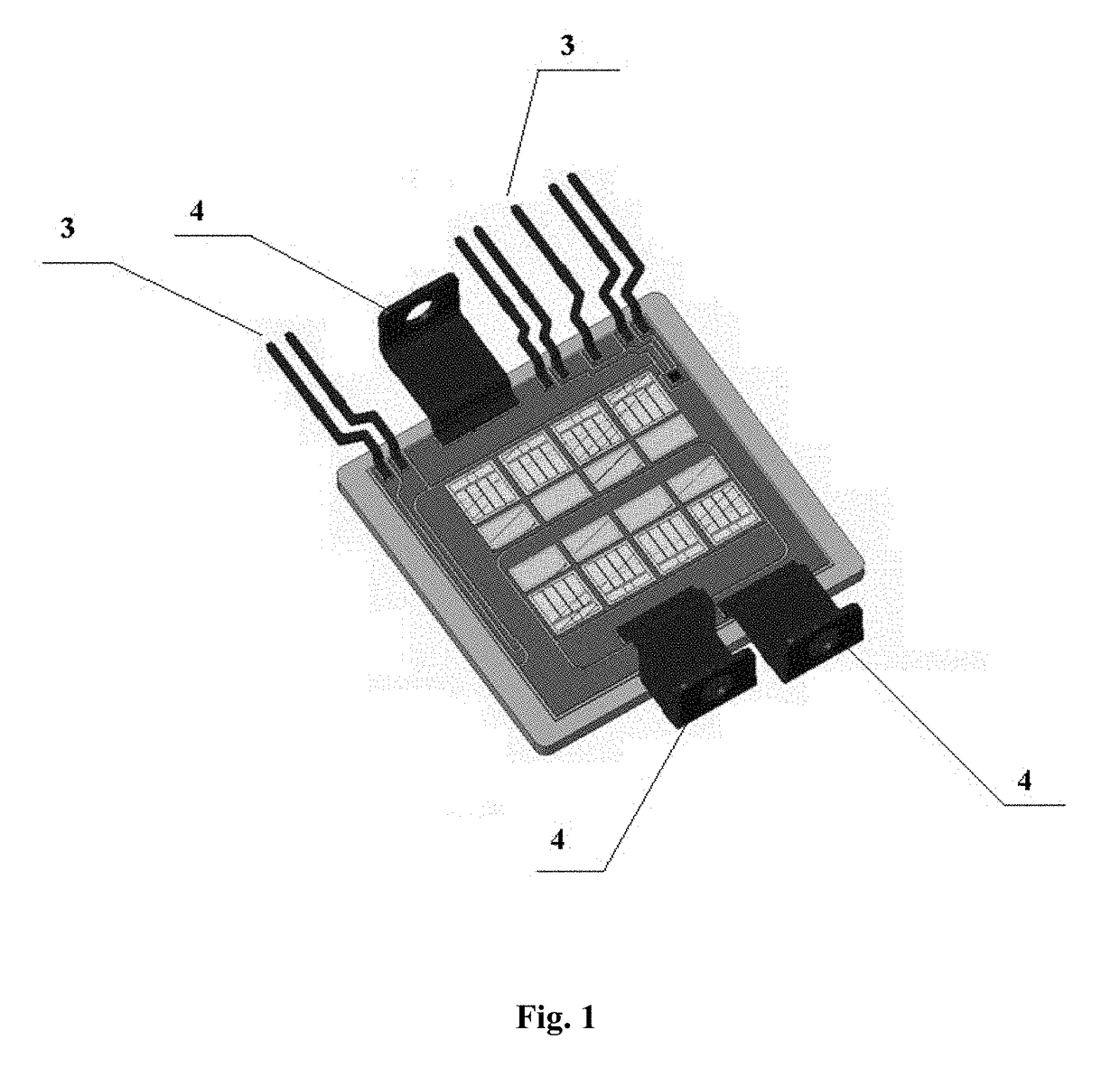
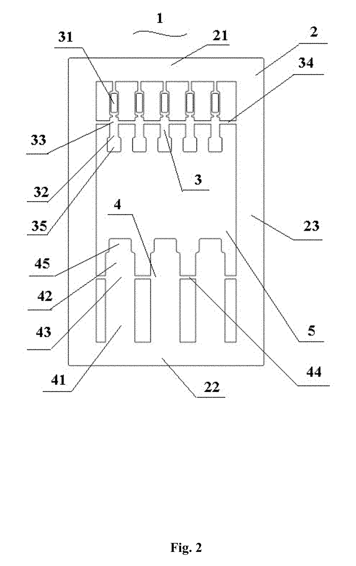
[0054]FIG. 3 is a schematic top view of an exemplary lead frame with a power sub lead frame and a control sub lead frame which are formed by different metallic materials in an exemplary embodiment of the invention, before placing onto a substrate of a power electronic device; and FIG. 4(a)-4(e) are schematic top views illustrating the method of attaching a semiconductor chip onto a substrate while forming individual final power terminals and control terminals, by using the exemplary lead frame in FIG. 3. The substrate 2022 may typically be formed from a direct copper bond (DCB) structure where a ceramic inner plate is covered with a copper layer on both sides. When used in a power module such as in the current invention, one of the copper layers may be used for the mounting of electrical components (and the lead frame), and this copper layer may be patterned to give track areas electrically insulated from other track areas.
[0055]According to a general technical...
embodiment i
Bimetallic Interface Embodiment I
[0066]FIG. 5(a) illustrates a partially enlarged schematic cross-sectional view of the lead frame as illustrated in FIG. 3, at its bimetallic interface 106 where the power sub lead frame 1012 and the control sub lead frame 1011 are bonded directly together, according to an embodiment of the present invention.
[0067]In an exemplary embodiment of the invention, the power sub lead frame 1012 formed by a metallic material, either a pure metal or its alloy, and the control sub lead frame 1011 which is formed by a different metallic material, are placed to abut directly and tightly against each other at ends and subsequently bonded / jointed together, e.g., by a number of available technologies including laser welding, ultrasonic welding, cladding, or use of epoxy resins, other welding means, or any other attaching means, to form the bimetallic interface 106. Hereby, the bimetallic interface 106 is defined along all abutting portions of the power sub lead fra...
embodiment ii
Bimetallic Interface Embodiment II
[0069]FIG. 5(b) illustrates a partially enlarged schematic cross-sectional view of the lead frame as illustrated in FIG. 3, at its bimetallic interface 106 where the power sub lead frame 1012 and the control sub lead frame 1011 are bonded together by inserting free end portions of one sub lead frame into the profiles of free end portions of another sub lead frames, according to another embodiment of the present invention.
[0070]The lead frame of the Bimetallic Interface Embodiment II as illustrated in FIG. 5(b) only differs from that of the Bimetallic Interface Embodiment I as illustrated in FIG. 5(a) in the specific structure at the bimetallic interface.
[0071]Alternatively, in an exemplary embodiment of the invention, the aforementioned bimetallic interface as in FIG. 5(a) is formed to abut each other at ends of the lateral beams directly. In contrast, as illustrated in FIG. 5(b), along the intended bimetallic interface, the ends of the lateral beam...
PUM
 Abstract
Description
Claims
Application Information


