Electroabsorption Modulator Integrated Distributed Feedback Laser with Integrated Semiconductor Optical Amplifier, and Driving Method for Same

a distributed feedback and semiconductor technology, applied in semiconductor lasers, semiconductor amplifier structures, instruments, etc., can solve the problems of difficult to acquire the optical power for long distance transmission, dfb laser optical power loss is largely lost, etc., and achieves low power consumption and high output power.

Active Publication Date: 2018-01-25
NIPPON TELEGRAPH & TELEPHONE CORP
View PDF9 Cites 1 Cited by
  • Summary
  • Abstract
  • Description
  • Claims
  • Application Information

AI Technical Summary

Benefits of technology

[0019]According to the present invention, it is possible to provide the SOA integrated EA-DFB laser that can realize the high output power, the low power consumption and the negative chirp value simultaneously in contrast to the conventional EA-DFB laser, and the driving method therefor.

Problems solved by technology

However, when the absolute value of the DC bias Vb is made large, a loss of the EA modulator increases to cause an optical power of light to be outputted from the DFB laser to be largely lost.
Therefore, in the conventional EA-DFB laser, it is difficult to acquire the optical power enough for the long distance transmission.

Method used


Image

  • Electroabsorption Modulator Integrated Distributed Feedback Laser with Integrated Semiconductor Optical Amplifier, and Driving Method for Same
  • Electroabsorption Modulator Integrated Distributed Feedback Laser with Integrated Semiconductor Optical Amplifier, and Driving Method for Same
  • Electroabsorption Modulator Integrated Distributed Feedback Laser with Integrated Semiconductor Optical Amplifier, and Driving Method for Same

Examples


first embodiment

[0054]By referring to Table 1, an SOA integrated EA-DFB laser according to a first embodiment of the present invention will be explained. Table 1 indicates characteristics of an EA-DFB laser and an SOA integrated EA-DFB laser in a case of driving the EA-DFB laser and the SOA integrated EA-DFB laser when a drive electric current of the EA-DFB laser is set to 80 mA, and in the SOA integrated EA-DFB laser an injection electric current IDFB into the DFB laser portion 12 is set to 60 mA, an SOA length LSOA is set to 50 μm, an operating temperature is set to 45° C. and an injection electric current ISOA into the SOA portion 13 is set to 10 mA or 25 mA. In Table 1, Pavg indicates an optical power, DER indicates a dynamic extinction ratio, OMA indicates an optical modulation power, f3 dB indicates a cutoff frequency in a band of 3 dB, and P indicates a power consumption.

TABLE 1EA-DFB laserSOA integrated EA-DFB laserIDFB [mA]8060ISOA [mA]—1025Pavg [dBm]3.65.35.6DER [dB]8.18.08.1OMA [dBm]5.36...

second embodiment

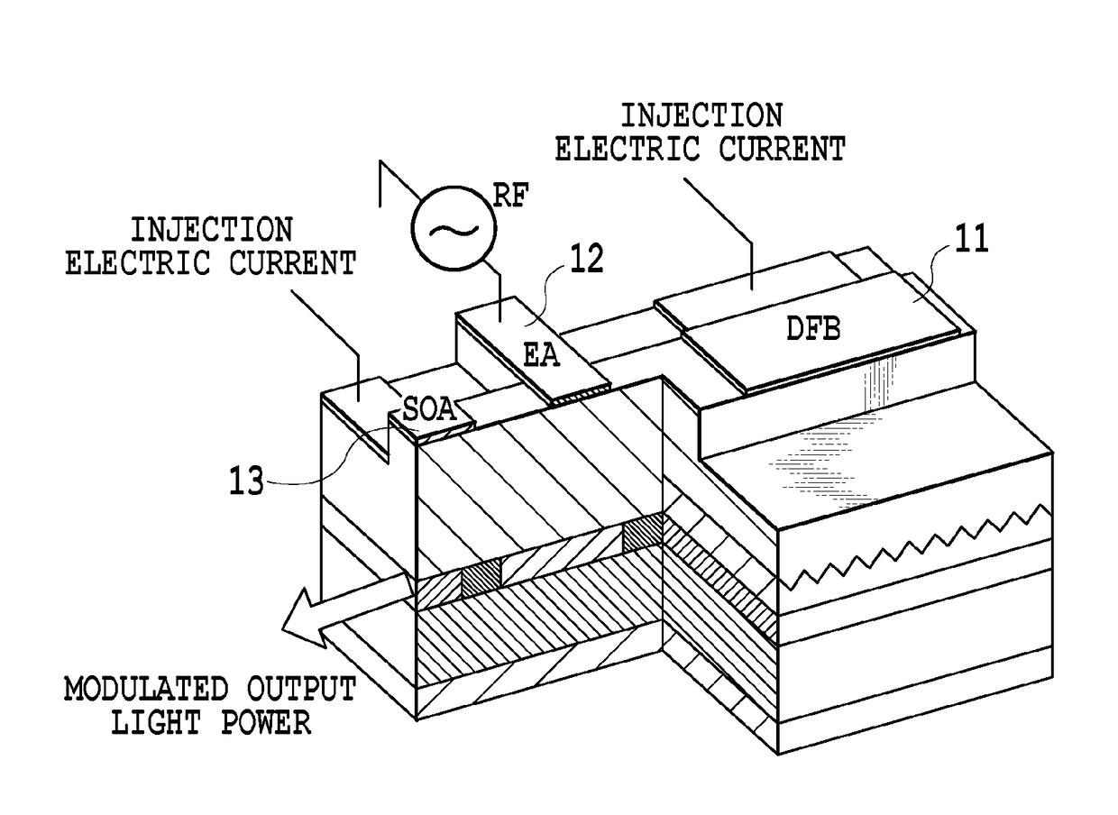
[0056]By referring to FIG. 9, an SOA integrated EA-DFB laser according to a second embodiment of the present invention will be explained. FIG. 9 indicates the SOA integrated EA-DFB laser in which the DFB laser portion 11, the EA-modulator portion 12 into which output light is input from the DFB laser portion 11 and the SOA portion 13 into which modulated output light modulated in and outputted from the EA modulator portion 12 is input for amplification are monolithically-integrated on a same substrate. As illustrated in FIG. 9, the DFB laser portion 11 and the SOA portion 13 are controlled using a same control terminal 14. A production process of the SOA integrated EA-DFB laser according to the second embodiment is indicated in PL 1, for example.

[0057]In the present embodiment, a length of the SOA portion 13 in regard to the optical waveguide direction is set to 50 μm, and a length of the DFB laser portion 11 in regard to the optical waveguide direction is set to 300 Since a ratio i...


PUM


Abstract

The present invention relates to a driving method for an SOA integrated EA-DFB laser monolithically-integrating a DFB laser portion, an EA modulator portion and an SOA portion, on a same substrate, wherein an electric current ISOA is injected into the SOA portion within a range of a power consumption not exceeding a total amount of a power consumption eliminated in the DFB laser portion of the SOA integrated EA-DFB laser and a power consumption eliminated in the EA modulator portion of the SOA integrated EA-DFB laser by eliminating an elimination amount ΔIDFB from a maximum injection electric current into a DFB laser portion of an EA-DFB laser allowable in a case of mounting the EA-DFB laser on an optical transmission module.

Description

TECHNICAL FIELD[0001]The present invention relates to an electroabsorption modulator integrated distributed feedback laser (EA-DFB) with an integrated semiconductor optical amplifier (SOA), and a driving method therefor.BACKGROUND ART[0002]Along with the widespread use of optical communications, speeding-up of a communication rate such as from 10 Gbit / s to 25 Gbit / s, further 40 Gbit / s is advancing in a metro optical communication network for connection of relay stations between cities. In this metro optical communication, for example, in a case of 10 Gbit / s, a long-distance transmission of 40 to 80 km transmission in a single mode fiber (SMF) is required (a transmission distance to be required reduces typically in inverse proportion to the square of a bit rate (modulation rate)), and it is an important task to achieve miniaturization, a low power consumption and a low chirp in an optical transmission module.[0003]External modulation systems low in a chirp are in general used for per...

Claims


Application Information

Patent Timeline
Patent Type & Authority Applications(United States)
IPC IPC(8): H01S5/042H01S5/0625H01S5/50H01S5/026H01S5/12
CPCH01S5/042H01S5/026H01S5/06253H01S5/50H01S5/12H01S5/0085H01S5/0265H01S5/0622G02F1/00H01S5/4031G02B6/12
Inventor KOBAYASHI, WATARUITO, TOSHIO
Owner NIPPON TELEGRAPH & TELEPHONE CORP
Why Eureka
Try Eureka