
Glass substrate including passive-on-glass device and semiconductor die

Active Publication Date: 2018-01-25
QUALCOMM INC
View PDF4 Cites 12 Cited by
  • Summary
  • Abstract
  • Description
  • Claims
  • Application Information

AI Technical Summary

Benefits of technology

The present disclosure relates to a device that includes a passive-on-glass (POG) device and a semiconductor die integrated inside a glass substrate. By doing so, the device may have a reduced thickness and weight as compared to devices that use a surface mount technology. The device also includes a three-dimensional inductor that improves device performance and increases component density by wrapping around the semiconductor die. The technical effects of the invention include reduced size and weight of the device, improved performance, and increased component density.

Problems solved by technology

In some circumstances, data received by an electronic device may be subject to noise or interference, which may reduce signal quality of the data or which may cause the data to be retransmitted.
Increasing a size of the glass substrate to accommodate the increased size or number of components may cause the glass substrate to deviate from a design specification, such as if the glass substrate becomes too large to be included in the mobile device.

Method used


Image

  • Glass substrate including passive-on-glass device and semiconductor die
  • Glass substrate including passive-on-glass device and semiconductor die
  • Glass substrate including passive-on-glass device and semiconductor die

Examples


Embodiment Construction

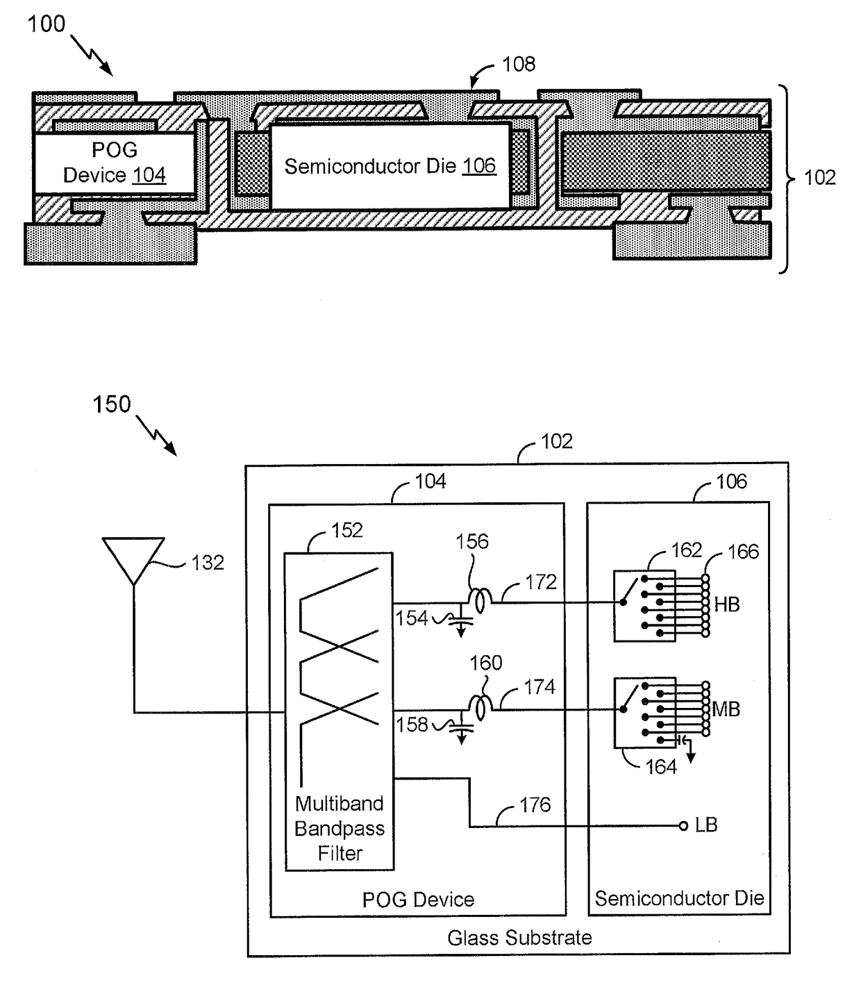
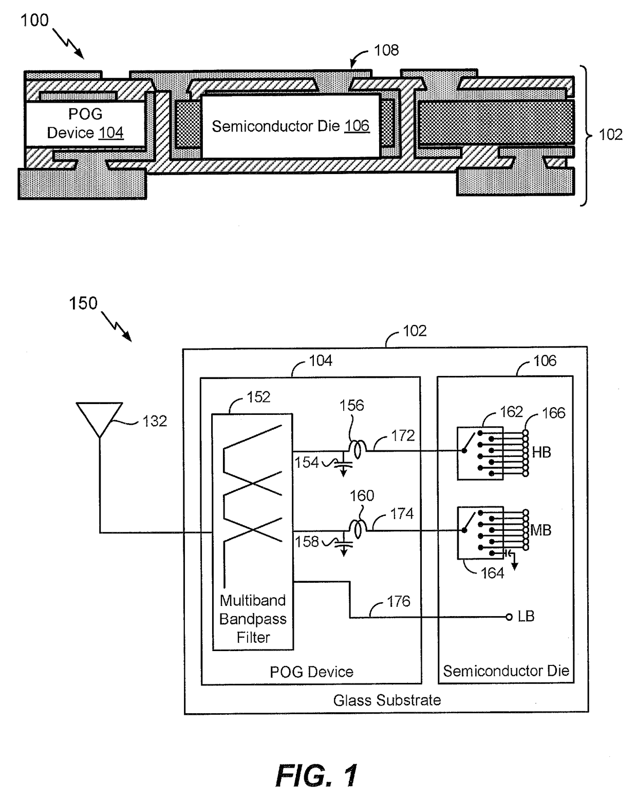
[0020]FIG. 1 illustrates a cross-sectional view 100 of a glass substrate 102. Depending on the particular implementation, the glass substrate 102 may correspond to a substrate of a package configured to enclose an integrated circuit, a substrate of an interposer configured to connect integrated circuits or an integrated circuit and a printed circuit board (PCB), or a substrate of a hybrid integrated circuit (HIC), as illustrative examples.

[0021]The glass substrate 102 includes a passive-on-glass (POG) device 104. The POG device 104 is integrated within the glass substrate 102. The POG device 104 may include one or more passive components, such as one or more inductors, one or more capacitors, a filter circuit (e.g., a bandpass filter circuit), one or more other components, or a combination thereof.

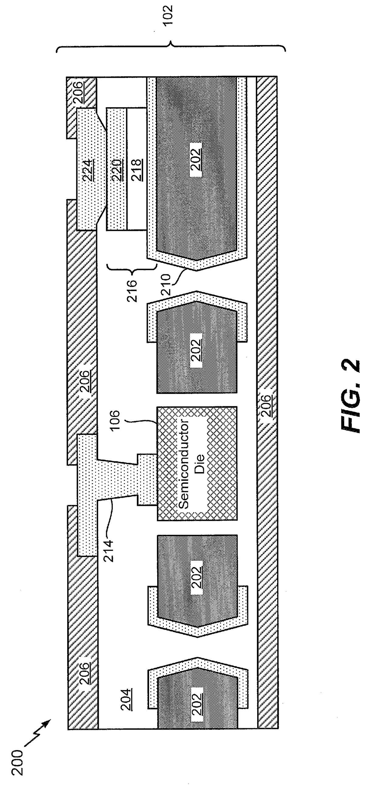
[0022]The glass substrate 102 also includes a semiconductor die 106 (e.g., a silicon semiconductor die). The semiconductor die 106 is integrated within the glass substrate 102. The semicon...


PUM


Abstract

In an illustrative example, an apparatus includes a passive-on-glass (POG) device integrated within a glass substrate. The apparatus further includes a semiconductor die integrated within the glass substrate.

Description

I. FIELD[0001]The present disclosure is generally related to electronic devices and more particularly to electronic devices that include glass substrates.II. DESCRIPTION OF RELATED ART[0002]Electronic devices include mobile devices, servers, base stations, and other devices that enable storage, retrieval, and processing of information. As an illustrative example, a server may communicate with a computer or other device using a wired network, such as a local area network (LAN) or the Internet. As another example, a mobile device may use a wireless network to communicate data with a base station or other device. In some circumstances, data received by an electronic device may be subject to noise or interference, which may reduce signal quality of the data or which may cause the data to be retransmitted.[0003]To improve quality of received signals, certain components of a mobile device may be formed on a glass substrate. For example, a circuit component may be formed on a glass substra...

Claims


Application Information

Patent Timeline
IPC IPC(8): H04B1/16H01L21/48H01L23/498H01L23/66H01L27/01H01L49/02
CPCH04B1/1638H01L27/01H01L28/40H01L28/10H01L23/49827H01L23/49838H01L2223/6688H01L21/4853H01L21/486H01L2223/6672H01L2223/6616H01L2223/6677H01L23/66H01F17/0013H01L23/64H01L24/19H01L24/20H01L2224/04105H01L2224/24195H01L2924/10253H01L2924/13091H01L2924/1421H01L2924/15153H01L2924/19041H01L2924/19042H01L2924/19105H03H7/0115H04B1/006H05K1/165H05K1/185H05K3/4605H05K2201/09536H05K2201/0959H05K2201/097H05K2201/09827H01L23/5223
Inventor YUN, CHANGHANZUO, CHENGJIEVELEZ, MARIOMUDAKATTE, NIRANJAN SUNILGU, SHIQUNKIM, JONGHAEBERDY, DAVID
Owner QUALCOMM INC
Learn More