Design for solid cells
a solid cell and cell layer technology, applied in the field of solid cell design, can solve the problems of high production cost, and achieve the effect of simplifying the connection arrangement of cell layers
- Summary
- Abstract
- Description
- Claims
- Application Information
AI Technical Summary
Benefits of technology
Problems solved by technology
Method used
Image
Examples
Embodiment Construction
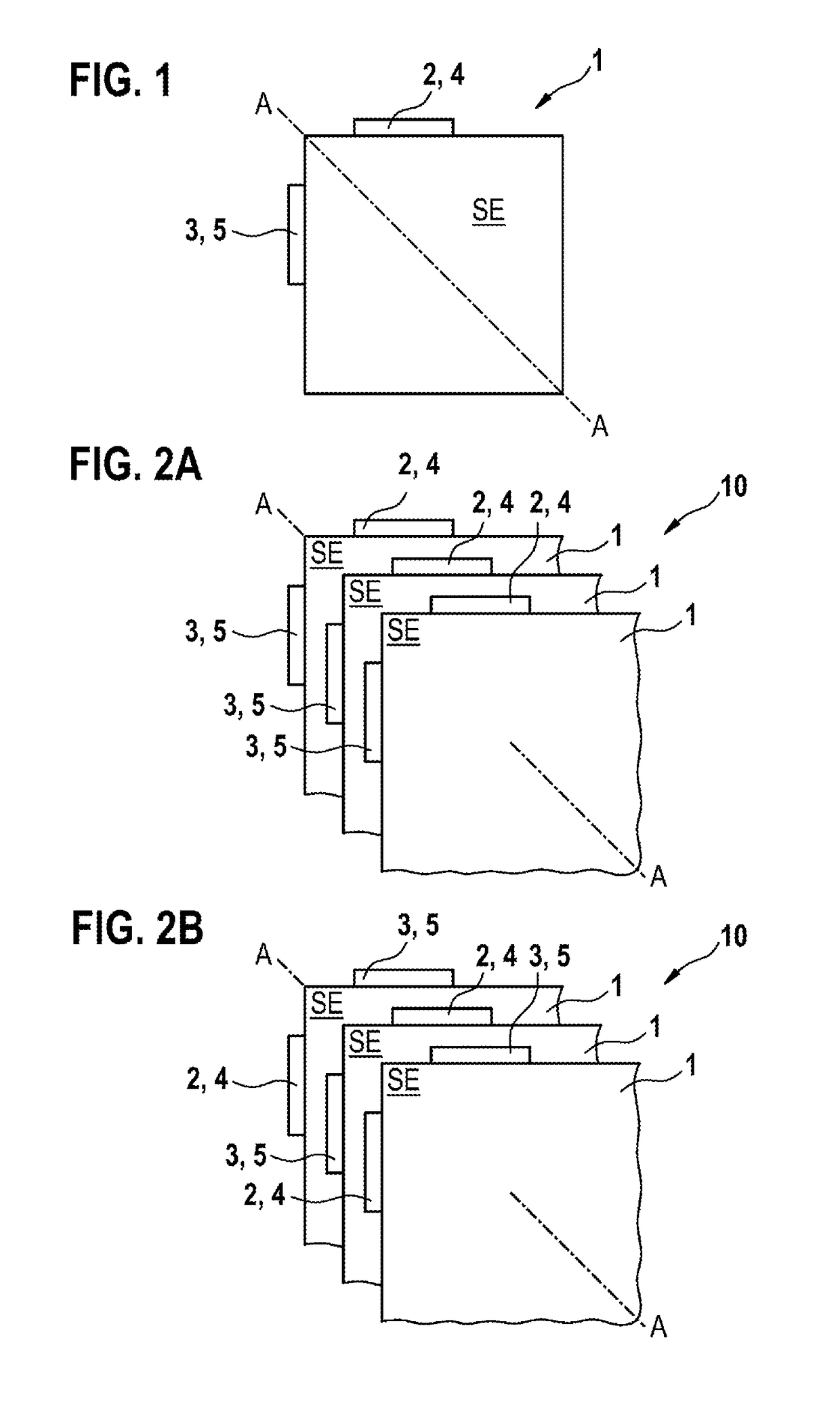
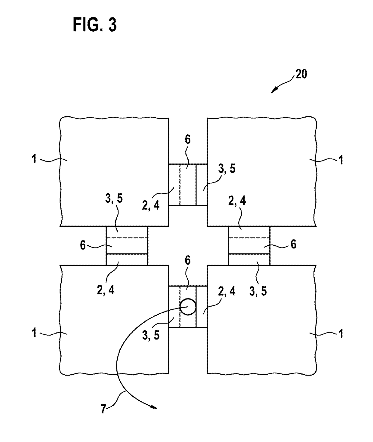
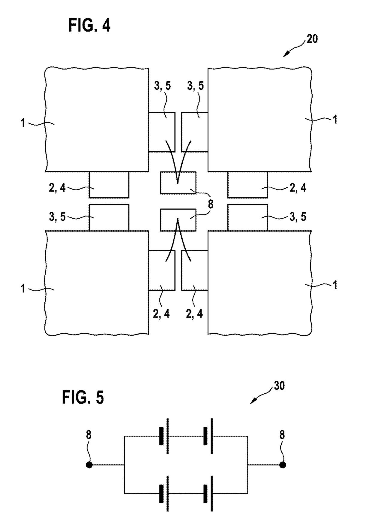
[0043]FIG. 1 illustrates a schematic view of a cell layer 1 when viewing the plane of symmetry SE from above, wherein the cell layer is embodied so as to produce a solid-state cell according to the method in accordance with the invention. The cell layer 1 comprises a first conductive layer 2 and a second conductive layer 3. The first conductive layer 2 is separated from the second conductive layer 3 at least by means of a separating layer (not illustrated here). The first conductive layer 2 is advantageously the cathode conductive layer that is preferably produced from an aluminum sheet. The second conductive layer 3 is advantageously the anode conductive layer, the material of which is embodied from a copper or nickel sheet material. The first conductive layer 2, namely in this case advantageously the aluminum sheet, is embodied in the form of a contact lug so as to form a current collector 4, the current collector 5 that in addition is embodied from the second conductive layer 3 i...
PUM
| Property | Measurement | Unit |
|---|---|---|
| shrinkage | aaaaa | aaaaa |
| axis of symmetry | aaaaa | aaaaa |
| symmetry | aaaaa | aaaaa |
Abstract
Description
Claims
Application Information


