Eureka AIR delivers breakthrough ideas for toughest innovation challenges, trusted by R&D personnel around the world.

Optical modulator using phase change material and device including the same

Active Publication Date: 2018-02-15
SAMSUNG ELECTRONICS CO LTD
View PDF3 Cites 7 Cited by
  • Summary
  • Abstract
  • Description
  • Claims
  • Application Information

AI Technical Summary

Benefits of technology

The patent text describes optical modulators that have simple structures and excellent performance. The modulators can reduce the thickness of the optical modulation layer and lower the operating voltage. Additionally, they can achieve high light modulation rates and high contrast ratios.

Problems solved by technology

However, in the group III-V compound semiconductor-based optical modulator, due to a thick absorption layer of about several micrometers or more and a complex stacked structure for improving performance, manufacturing process may become more complex, reproducibility of a device may be lowered, and manufacturing costs may be increased.

Method used


Image

  • Optical modulator using phase change material and device including the same
  • Optical modulator using phase change material and device including the same
  • Optical modulator using phase change material and device including the same

Examples


Embodiment Construction

[0075]Various example embodiments will now be described more fully with reference to the accompanying drawings in which example embodiments are shown.

[0076]It will be understood that when an element is referred to as being “connected” or “coupled” to another element, it can be directly connected or coupled to the other element or intervening elements may be present. In contrast, when an element is referred to as being “directly connected” or “directly coupled” to another element, there are no intervening elements present. As used herein the term “and / or” includes any and all combinations of one or more of the associated listed items.

[0077]It will be understood that, although the terms “first,”“second,” etc. may be used herein to describe various elements, components, regions, layers and / or sections, these elements, components, regions, layers and / or sections should not be limited by these terms. These terms are only used to distinguish one element, component, region, layer or sectio...


PUM


Abstract

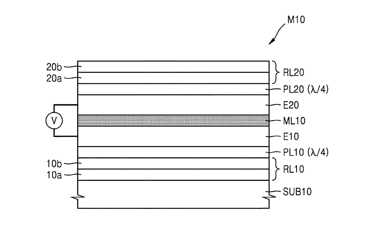
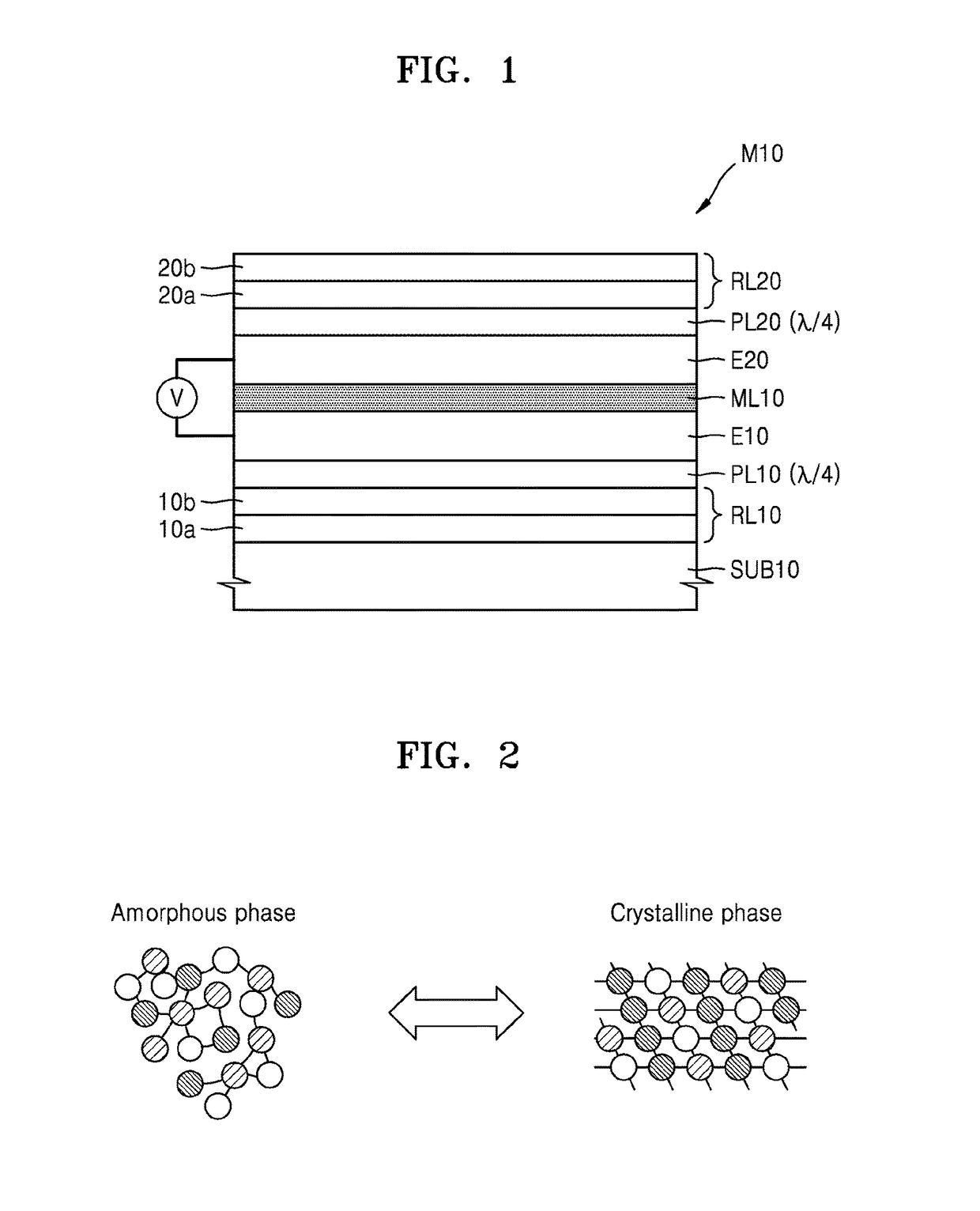
Provided are optical modulators and devices including the optical modulators. The optical modulator may include an optical modulation layer that includes a phase change material. A first electrode may be provided on a first surface of the optical modulation layer. A second electrode may be provided on a second surface of the optical modulation layer. A first phase controlling layer may be provided, the first electrode being disposed between the first phase controlling layer and the optical modulation layer. A second phase controlling layer may be provided, the second electrode being disposed between the second phase controlling layer and the optical modulation layer. Each of the first and the second phase controlling layers may have an optical thickness corresponding to an odd multiple of λ / 4, where λ is a wavelength of incident light to be modulated by the optical modulator. The optical modulator may further include at least one reflective layer. The optical modulation layer may have a thickness of about 10 nm or less. An operating voltage of the optical modulator may be about 10 V or less.

Description

CROSS-REFERENCE TO RELATED APPLICATIONS[0001]This application claims priority from Korean Patent Application No. 10-2016-0101887, filed on Aug. 10, 2016, and Korean Patent Application No. 10-2016-0154888, filed on Nov. 21, 2016, in the Korean Intellectual Property Office, the disclosures of which are incorporated herein in their entireties by reference.BACKGROUND1. Field[0002]The present disclosure relates to optical modulators and devices including the optical modulators.2. Description of the Related Art[0003]Three-dimensional (3D) cameras are capable of measuring a distance from a plurality of points on a surface of an object to the 3D camera, in addition to having a photographing function. Various algorithms to measure a distance between an object and a 3D camera have been suggested and a Time-of-Flight (TOF) method is mainly in use. The TOF method is a method of measuring a flight time after illumination light is irradiated to an object and until the illumination light reflected...

Claims


Application Information

Patent Timeline
IPC IPC(8): G02F1/19H04B10/80H04B10/67G02F1/055H04B10/548
CPCG02F1/19G02F1/0553H04B10/548H04B10/67H04B10/80G02F2001/0151G02F2202/00G02F2203/50G02F1/0063G02F1/0126G02F1/0147G02F1/21G02F2201/346G02F2202/32G02F1/0151
Inventor NA, BYUNGHOONPARK, YONGHWA
Owner SAMSUNG ELECTRONICS CO LTD
Why Eureka
Eureka Blog
Learn More