
Material for forming underlayer film for lithography, composition for forming underlayer film for lithography, underlayer film for lithography, resist pattern forming method, and circuit pattern forming method

a technology of resist pattern and film thickness, which is applied in the direction of photosensitive material processing, photomechanical equipment, instruments, etc., can solve the problems of difficult to achieve resist pattern having a film thickness sufficient for processing a substrate, and the intrinsic limitation of light source resolution, so as to achieve excellent heat resistance and etching resistance

Inactive Publication Date: 2018-02-22
MITSUBISHI GAS CHEM CO INC
View PDF1 Cites 1 Cited by
  • Summary
  • Abstract
  • Description
  • Claims
  • Application Information

AI Technical Summary

Benefits of technology

The patent describes a material that can be used to create a layer that helps with the process of creating patterns in a computer chip. This material can be applied to a wet process and is good at withstanding heat and etching.

Problems solved by technology

In lithography using exposure to light, which is currently used as a general-purpose technique, the resolution is now approaching the intrinsic limitation associated with the wavelength of the light source.
However, as the resist pattern is made finer and finer, there arise a problem of resolution and a problem of collapse of the resist pattern after development, and therefore there is demanded for making a resist film thinner.
If the resist film is merely made thinner, however, it is difficult to achieve the resist pattern having a film thickness sufficient for processing a substrate.

Method used


Image

  • Material for forming underlayer film for lithography, composition for forming underlayer film for lithography, underlayer film for lithography, resist pattern forming method, and circuit pattern forming method
  • Material for forming underlayer film for lithography, composition for forming underlayer film for lithography, underlayer film for lithography, resist pattern forming method, and circuit pattern forming method
  • Material for forming underlayer film for lithography, composition for forming underlayer film for lithography, underlayer film for lithography, resist pattern forming method, and circuit pattern forming method

Examples


examples

[0193]Hereinafter, the present embodiment will be described in more detail by Synthesis Examples, Examples and Comparative Examples, but the present embodiment is not limited thereto at all.

[0194][Carbon Concentration and Oxygen Concentration]

[0195]The carbon concentration and the oxygen concentration (% by mass) were measured by organic element analysis with the following apparatus.

[0196]Apparatus: CHN CORDER MT-6 (trade name, manufactured by Yanaco Bunseki Kogyo Co.)

[0197][Weight Average Molecular Weight]

[0198]Gel permeation chromatography (GPC) analysis with the following apparatus and the like was used to determine the weight average molecular weight (Mw) in terms of polystyrene.

[0199]Apparatus: Shodex GPC-101 type (trade name, manufactured by Showa Denko K. K.)

[0200]Column: KF-80M×3

[0201]Eluent: THF 1 mL / min

[0202]Temperature: 40° C.

[0203][Solubility]

[0204]The amount of the compound dissolved in propylene glycol monomethyl ether acetate (PGMEA) was measured at 23° C., and the re...

example 3

[0237]The composition for forming an underlayer film for lithography in Example 1 was coated on a SiO2 substrate having a film thickness of 300 nm, and baked at 240° C. for 60 seconds and further at 400° C. for 120 seconds to thereby form an underlayer film having a film thickness of 70 nm. A resist solution for ArF was coated on the underlayer film, and baked at 130° C. for 60 seconds to thereby form a photoresist layer having a film thickness of 140 nm. As the resist solution for ArF, one prepared by blending 5 parts by mass of the compound of the following formula (12), 1 part by mass of triphenylsulfonium nonafluoromethanesulfonate, 2 parts by mass of tributylamine, and 92 parts by mass of PGMEA was used.

[0238]A compound of following formula (12) was prepared as follows. That is, 4.15 g of 2-methyl-2-methacryloyloxyadamantane, 3.00 g of methacryloyloxy-γ-butyrolactone, 2.08 g of 3-hydroxy-1-adamantyl methacrylate and 0.38 g of azobisisobutyronitrile were dissolved in 80 mL of te...

example 4

[0240]Except that the composition for forming an underlayer film for lithography in Example 2 was used instead of the composition for forming an underlayer film for lithography in Example 1, the same manner as in Example 3 was performed to provide a positive-type resist pattern. The evaluation results are shown in Table 2.


PUM

PropertyMeasurementUnit
temperatureaaaaaaaaaa
reaction timeaaaaaaaaaa

Abstract

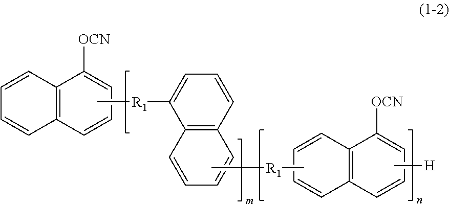
The present invention provides a material for forming an underlayer film for lithography, including a cyanic acid ester compound obtained by cyanation of a modified naphthalene formaldehyde resin.

Description

TECHNICAL FIELD[0001]The present invention relates to a material for forming an underlayer film for lithography, a composition for forming an underlayer film for lithography, an underlayer film for lithography, a resist pattern forming method, and a circuit pattern forming method.BACKGROUND ART[0002]Semiconductor devices are manufactured through microfabrication by lithography using a photoresist material, but are required to be made finer by a pattern rule in accordance with the increase in integration degree and the increase in speed of LSI in recent years. In lithography using exposure to light, which is currently used as a general-purpose technique, the resolution is now approaching the intrinsic limitation associated with the wavelength of the light source.[0003]A light source for lithography, for use in forming a resist pattern, has a shorter wavelength from a KrF excimer laser (248 nm) to an ArF excimer laser (193 nm). However, as the resist pattern is made finer and finer, t...

Claims


Application Information

Patent Timeline
Patent Type & Authority Applications(United States)
IPC IPC(8): G03F7/11H01L21/027
CPCH01L21/0276G03F7/30G03F7/11G03F7/162G03F7/20C08G14/12G03F7/40H01L21/027C08G73/0644G03F7/004G03F7/038G03F7/039G03F7/2004
Inventor OKADA, KANAMAKINOSHIMA, TAKASHIECHIGO, MASATOSHIHIGASHIHARA, GOOKOSHI, ATSUSHI
Owner MITSUBISHI GAS CHEM CO INC
Learn More