

Compound, material for forming underlayer film for lithography, underlayer film for lithography and pattern forming method
a technology of applied in the field of compound, material for lithography and underlayer film for lithography, and pattern forming methods, can solve the problems of high solvent solubility, and achieve the effect of excellent heat resistance and etching resistan
- Summary
- Abstract
- Description
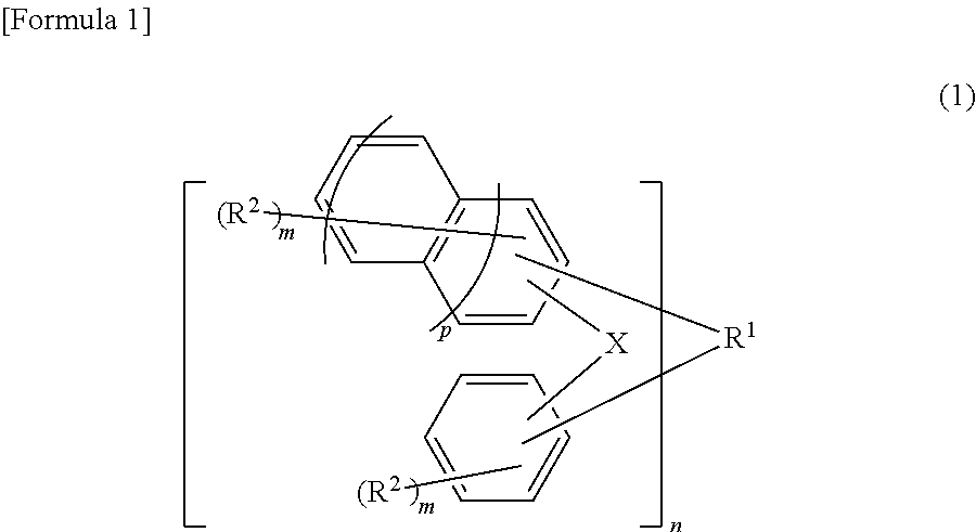
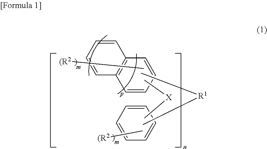
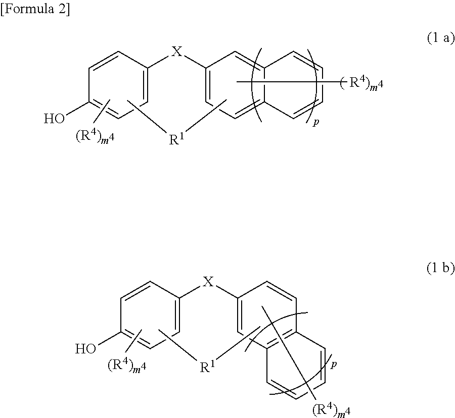
- Claims
- Application Information
AI Technical Summary
Benefits of technology
Problems solved by technology
Method used
Image

Examples
production example 1
[0194]A four-neck flask having a bottom outlet and an inner volume of 10 L, equipped with a Dimroth condenser, a thermometer and a stirring blade, was prepared. To this four-neck flask were charged 1.09 kg of 1,5-dimethylnaphthalene (7 mol, produced by Mitsubishi Gas Chemical Company, Inc.), 2.1 kg of a 40% by mass aqueous formalin solution (28 mol as formaldehyde, produced by Mitsubishi Gas Chemical Company, Inc.) and 0.97 ml of 98% by mass sulfuric acid (produced by Kanto Chemical Co., Inc.) under a nitrogen stream, and allowed the reaction to run under ordinary pressure with refluxing at 100° C. for 7 hours. Thereafter, ethylbenzene (special grade chemical, produced by Wako Pure Chemical Industries, Ltd.) (1.8 kg) as a dilution solvent was added to the reaction solution and left to stand, and then an aqueous phase being a bottom phase was removed. Furthermore, the resultant was neutralized and washed with water, and ethylbenzene and the unreacted 1,5-dimethylnaphthalene were dist...
example 2
[0219]Then, the solution of the material for forming an underlayer film for lithography in each of Example 1 was coated on a SiO2 substrate having a film thickness of 300 nm, and baked at 240° C. for 60 seconds and further at 400° C. for 120 seconds to thereby form an underlayer film having a film thickness of 80 nm. A resist solution for ArF was coated on the underlayer film, and baked at 130° C. for 60 seconds to thereby form a photoresist layer having a film thickness of 150 nm. Herein, as the resist solution for ArF, one prepared by blending 5 parts by mass of the compound of the following formula (11), 1 part by mass of triphenylsulfonium nonafluoromethanesulfonate, 2 parts by mass of tributylamine, and 92 parts by mass of PGMEA was used.
[0220]Herein, the compound represented by the following formula (11) was prepared as follows. That is, 4.15 g of 2-methyl-2-methacryloyloxyadamantane, 3.00 g of methacryloyloxy-γ-butyrolactone, 2.08 g of 3-hydroxy-1-adamantyl methacrylate and 0...
example 3
[0227]The solution of the material for forming an underlayer film for lithography in each of Example 1 was coated on a SiO2 substrate having a film thickness of 300 nm. Then, the solution of the material coated on the substrate was baked at 240° C. for 60 seconds and further at 400° C. for 120 seconds to thereby form an underlayer film having a film thickness of 80 nm. A silicon-containing intermediate layer material was coated on the underlayer film, and baked at 200° C. for 60 seconds to thereby form an intermediate layer film having a film thickness of 35 nm. Furthermore, the resist solution for ArF used in Example 2 was coated on the intermediate layer film, and baked at 130° C. for 60 seconds to thereby form a photoresist layer having a film thickness of 150 nm. Herein, as the silicon-containing intermediate layer material, a silicon atom-containing polymer described in in Japanese Patent Laid-Open No. 2007-226170 was used.
[0228]Then, the photoresist layer was exposed by using...
PUM
| Property | Measurement | Unit |
|---|---|---|
| temperature | aaaaa | aaaaa |
| temperature | aaaaa | aaaaa |
| temperature | aaaaa | aaaaa |
Abstract
Description
Claims
Application Information