Wireless module

a wireless module and wireless technology, applied in the direction of resonant antennas, individually energised antenna arrays, coupling device connections, etc., can solve the problem of difficult to reduce the thickness of wireless modules, and achieve the effect of widening the band increasing the impedance of the first antenna elemen

Inactive Publication Date: 2018-02-22
MURATA MFG CO LTD
View PDF14 Cites 13 Cited by
  • Summary
  • Abstract
  • Description
  • Claims
  • Application Information

AI Technical Summary

Benefits of technology

[0007]In the thickness direction of the dielectric board, a portion occupied by an antenna device including the first antenna element and the ground plane and a portion occupied by the shield member partially overlap each other. Therefore, it is possible to reduce the thickness of the wireless module as compared to a configuration in which the antenna device and the shield member are stacked in the thickness direction. Here, the resonant wavelength means an effective wavelength that takes into consideration the dielectric constant of the space between the first antenna element and the shield member, in the frequency band in which the first antenna element resonates.
[0009]It is possible to shield the high-frequency integrated circuit element by the ground plane and the shield member.
[0011]By operating either the first antenna element or the second antenna element, it is possible to switch the direction of strong directivity.
[0013]At a portion where the patch antenna and the shield member overlap each other, the patch antenna and the shield member capacitively couple to each other. Therefore, the amount of radio waves radiated from the edge of the patch antenna that overlaps with the shield member is smaller than the amount of radio waves radiated from the edge of the patch antenna that does not overlap the shield member. As a result, it is possible to regard the patch antenna approximately as one wave source, and thus it is possible to achieve wider directivity.
[0015]It is possible to reduce the thickness of the wireless module as compared to a configuration in which a monopole antenna is stacked on the shield member.
[0017]Since the first antenna element operates as a folded monopole antenna, it is possible to increase the impedance of the first antenna element and widen the band of the first antenna element.

Problems solved by technology

In the thickness direction of the board, since an antenna device including the antenna conductor and the shield electrode (ground) is stacked on a portion from the upper surface of the board to the shield electrode in which portion the high-frequency integrated circuit element is housed, it is difficult to reduce the thickness of the wireless module.

Method used


Image

  • Wireless module
  • Wireless module
  • Wireless module

Examples


first embodiment

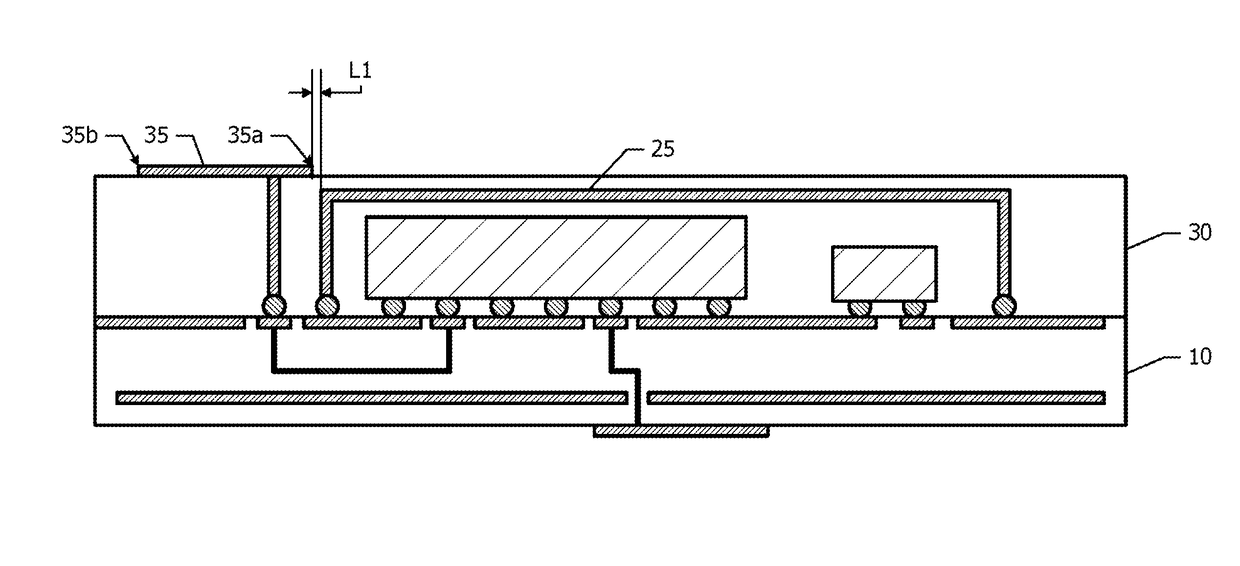
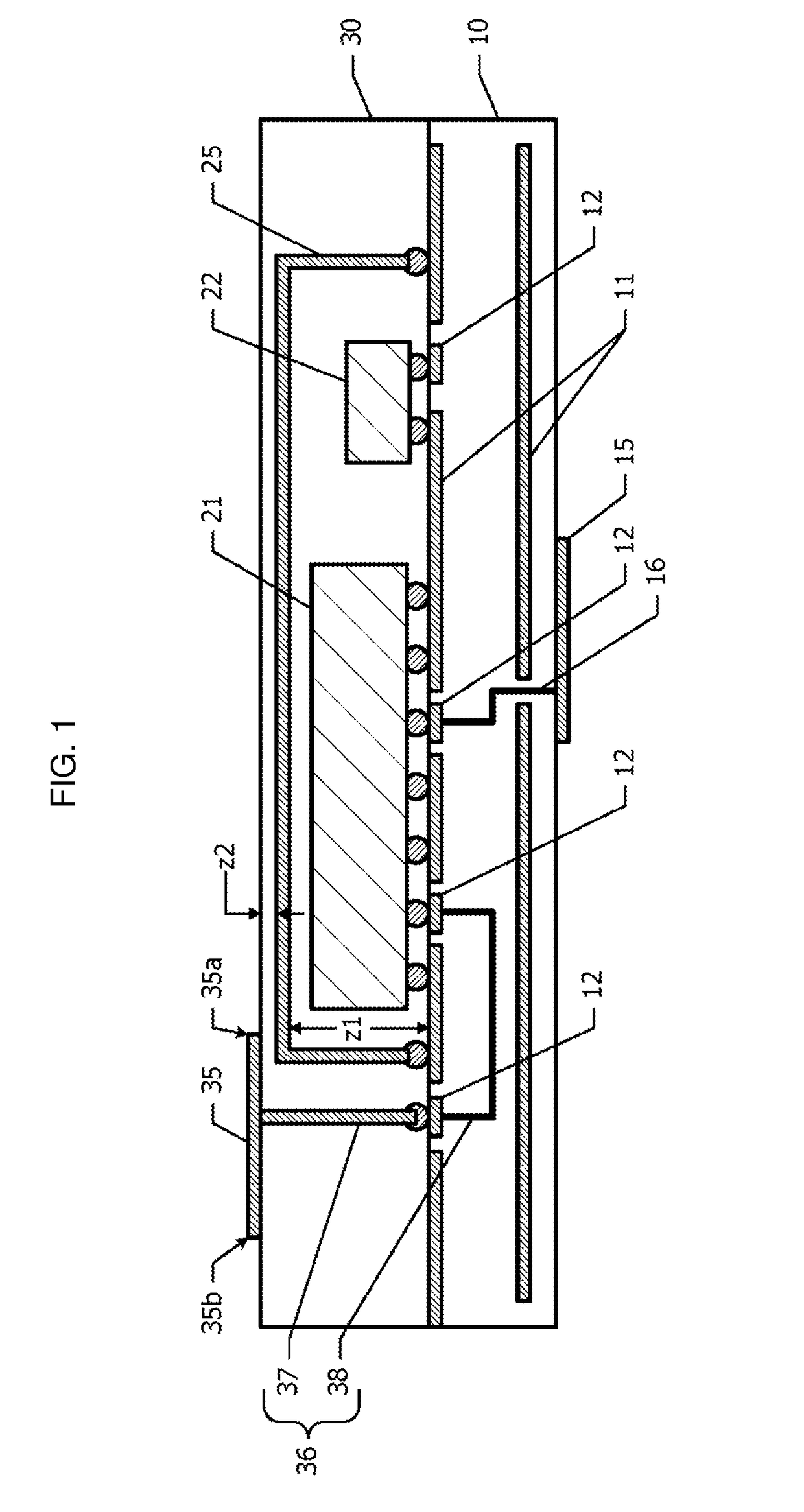
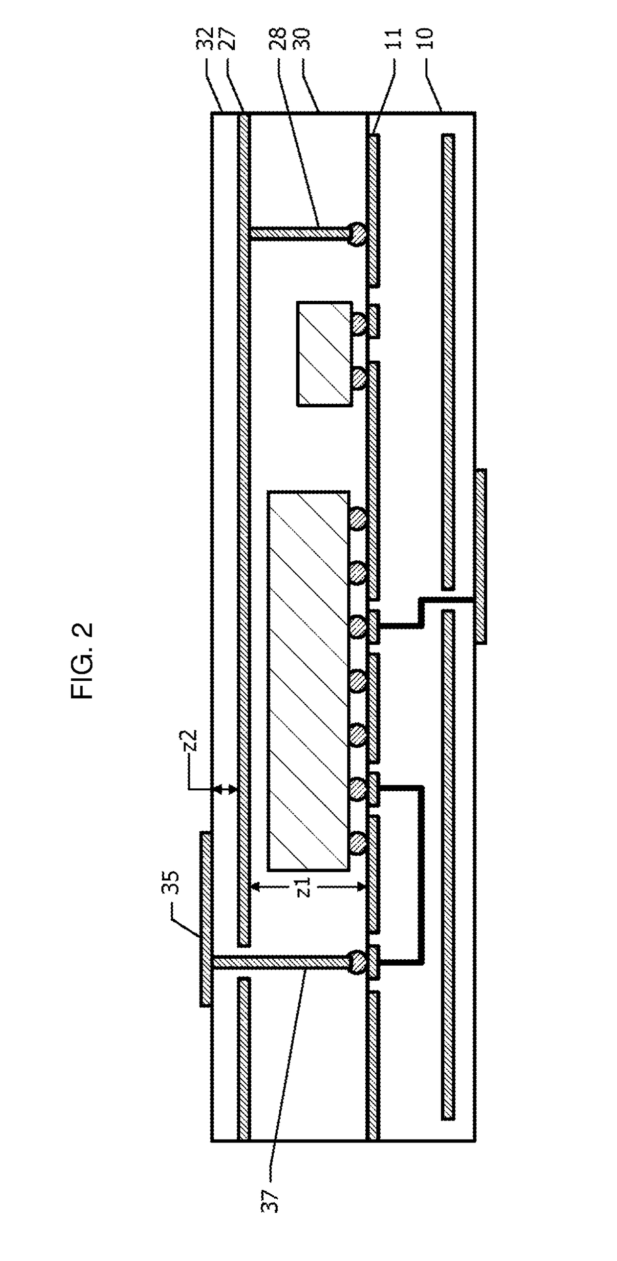
[0025]A wireless module according to a first embodiment will be described with reference to FIG. 1.

[0026]FIG. 1 is a schematic cross-sectional view of the wireless module according to the first embodiment. Ground planes 11 are provided to a dielectric board 10. The ground planes 11 may be disposed only within the dielectric board 10, or may be disposed both on the surface of the dielectric board 10 and within the dielectric board 10. FIG. 1 shows an example in which the ground planes 11 are disposed on the upper surface of the dielectric board 10 and within the dielectric board 10. A partial region of the ground plane 11 disposed on the upper surface is used as a ground land. Furthermore, signal lands 12 are provided on the upper surface of the dielectric board 10.

[0027]A high-frequency integrated circuit element 21 and a passive component 22 are mounted on the upper surface of the dielectric board 10. Part of terminals of the high-frequency integrated circuit element 21 is connecte...

second embodiment

[0047]Next, a wireless module according to a second embodiment will be described with reference to FIG. 3. Hereinafter, the difference from the first embodiment shown in FIG. 1 will be described, and the description of the configuration common with the first embodiment is omitted.

[0048]FIG. 3 is a schematic diagram of the wireless module according to the second embodiment. In the first embodiment, a portion of the first antenna element 35 overlaps with the shield member 25 in a plan view. However, in the second embodiment, the entire range of the first antenna element 35 is disposed outside the shield member 25 in a plan view. When the spaced distance from the shield member 25 to the first antenna element 35 in an in-plane direction is represented by L1, the spaced distance L1 is not smaller than about 0.

[0049]The positional relationship between the outer edge 35b of the first antenna element 35 and the ground plane 11 is the same as that in the first embodiment. Unlike the structur...

third embodiment

[0051]Next, a wireless module according to a third embodiment will be described with reference to FIG. 4. Hereinafter, the difference from the wireless module according to the first embodiment shown in FIG. 1 will be described, and the description of the configuration common with the wireless module according to the first embodiment is omitted.

[0052]FIG. 4 shows a plan view of the wireless module according to the third embodiment. The first antenna element 35 is disposed on the upper surface of the sealing member 30. The first antenna element 35 has a patch array antenna structure in which a plurality of radiation electrodes 39 are aligned in a row. Each radiation electrode 39 has a substantially square or rectangular planar shape. In a plan view, one edge 39a of each radiation electrode 39 is disposed inside the shield member 25, and an edge 39b opposing to the edge 39a is disposed outside the shield member 25. The other two edges intersect with the contour line of the shield membe...


PUM


Abstract

A ground plane is provided to a dielectric board. A high-frequency integrated circuit element is mounted on the dielectric board. A shield member electromagnetically shielding the high-frequency integrated circuit element is provided on the dielectric board. A first antenna element is provided on the dielectric board and at the same side as the shield member with respect to the ground plane. The first antenna element is connected to the high-frequency integrated circuit element by a first feed line. In a plan view, a portion of the first antenna element is disposed outside the shield member, a remaining portion of the first antenna element overlaps the shield member, or an entire range of the first antenna element is disposed outside the shield member, and a spaced distance from the shield member to the first antenna element is not greater than about ½ of a resonant wavelength of the first antenna element.

Description

[0001]This application claims priority from Japanese Patent Application No. 2016-161614 filed on Aug. 22, 2016. The content of this application is incorporated herein by reference in its entirety.BACKGROUND OF THE DISCLOSURE1. Field of the Disclosure[0002]The present disclosure relates to a wireless module.2. Description of the Related Art[0003]A high-frequency wireless module obtained by modularizing an antenna element, a passive element, and a high-frequency integrated circuit element having a transmission / reception function in a high-frequency band, is publicly known (Japanese Unexamined Patent Application Publication No. 2007-129304). For example, electronic components such as a high-frequency integrated circuit element and a passive element are mounted on a board and sealed by a sealing member. A shield electrode is provided within the sealing member, and an antenna conductor such as a patch antenna is provided on the upper surface of the sealing member. The shield electrode fo...

Claims


Application Information

Patent Timeline
Patent Type & Authority Applications(United States)
IPC IPC(8): H01L23/66H01Q9/40H01Q9/06H01Q9/04H01R12/72H01R24/50
CPCH01L23/66H01Q9/40H01Q9/065H01Q9/0485H01R12/722H01R24/50H01Q9/0407H01L2924/142H01L23/552H01Q1/2283H01Q1/38H01Q1/526H01Q9/0457H01Q9/30H01Q21/08H01Q21/28H01L2223/6677H01L2224/16227H01L2924/15192H01L2924/15313H01L2924/19105H01L2924/3025
Inventor UEDA, HIDEKI
Owner MURATA MFG CO LTD
Why Eureka
Try Eureka