Eureka AIR delivers breakthrough ideas for toughest innovation challenges, trusted by R&D personnel around the world.

Nonvolatile memory and a nonvolatile memory system

Active Publication Date: 2018-03-01
SAMSUNG ELECTRONICS CO LTD
View PDF3 Cites 6 Cited by
  • Summary
  • Abstract
  • Description
  • Claims
  • Application Information

AI Technical Summary

Benefits of technology

The patent describes a nonvolatile memory and memory system that can change how they manage data based on a change in power supply. This is accomplished through a control logic that uses a page management unit to determine whether to clear or maintain individual pieces of data based on a set flag corresponding to each piece of data. The technical effect of this invention is that it allows for more efficient management of data in nonvolatile memory, improving its performance and reliability.

Problems solved by technology

The volatile memory device loses stored data when it is powered-off.
In addition, data stored in the volatile main memory is lost during power-off.

Method used


Image

  • Nonvolatile memory and a nonvolatile memory system
  • Nonvolatile memory and a nonvolatile memory system
  • Nonvolatile memory and a nonvolatile memory system

Examples


Embodiment Construction

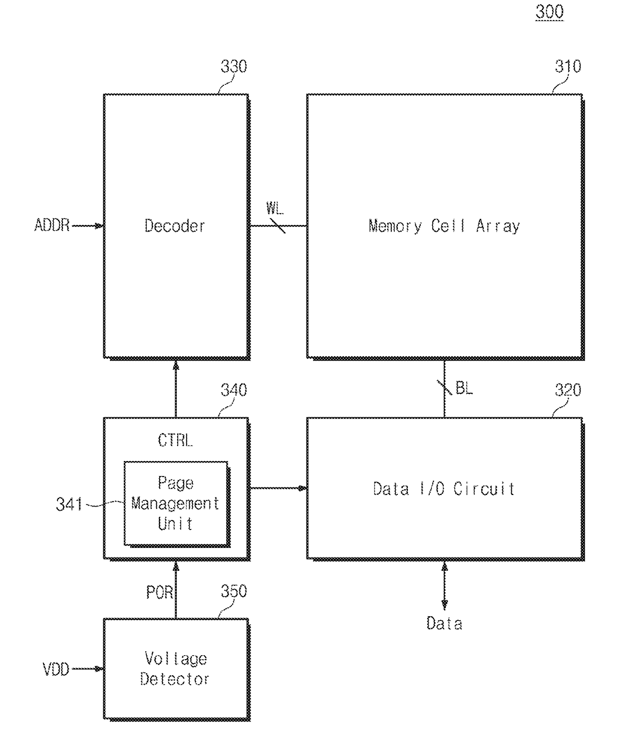
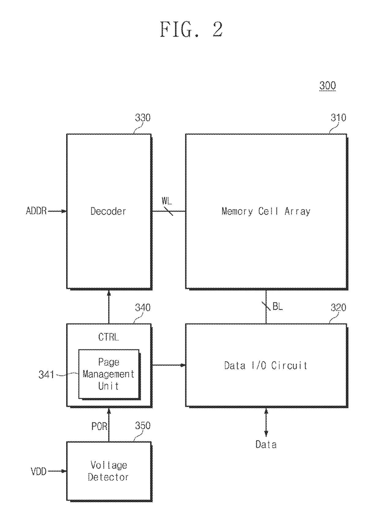
[0017]Below, exemplary embodiments of the inventive concept will be described more fully with reference to the accompanying drawings. In the drawings, like reference numerals may refer to like parts.

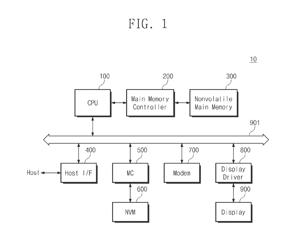
[0018]FIG. 1 is a block diagram illustrating a memory system 10, according to an exemplary embodiment of the inventive concept.

[0019]Referring to FIG. 1, the memory system 10 includes a central processing unit (CPU) 100, a main memory controller 200, a nonvolatile main memory 300, a host interface 400, a memory controller 500, a nonvolatile memory 600, a modem 700, a display driver 800, and a display 900.

[0020]The memory system 10 may allow the CPU 100, the main memory controller 200, the host interface 400, the memory controller 500, the modem 700, and the display driver 800 to exchange data with each other through a system bus 901. Data that is provided through the host interface 400 or processed by the CPU 100 is stored in the nonvolatile main memory 300.

[0021]The CPU 100 controls ove...


PUM


Abstract

A nonvolatile memory including: a memory cell array including a plurality of nonvolatile memory cells; a decoder connected to the memory cell array through a plurality of word lines; a data input / output (I / O) circuit connected to the memory cell array through a plurality of bit lines; and control logic configured to control the decoder and the data I / O circuit in response to a change in a power supply voltage to clear or maintain individual pieces of page data. The control logic includes a page management unit that determines whether to clear data included in the individual pieces of page data based on a value of a set flag respectively corresponding to the individual pieces of page data.

Description

CROSS-REFERENCE TO RELATED APPLICATION[0001]This application claims priority under 35 U.S.C. §119 to Korean Patent Application No. 10-2016-0110182 filed Aug. 29, 2016, in the Korean Intellectual Property Office, the disclosure of which is incorporated by reference herein in its entirety.TECHNICAL FIELD[0002]The inventive concept described herein relates to a memory device, and more particularly, to a nonvolatile memory and a nonvolatile memory system.DISCUSSION OF RELATED ART[0003]A semiconductor memory may be implemented by using a semiconductor such as silicon (Si), germanium (Ge), gallium arsenide (GaAs), and / or indium phosphide (InP), for example. Semiconductor memory devices may be classified as a volatile memory device or a nonvolatile memory device.[0004]The volatile memory device loses stored data when it is powered-off. The volatile memory device includes a static random access memory (SRAM), a dynamic RAM (DRAM), a synchronous DRAM, and the like. The nonvolatile memory dev...

Claims


Application Information

Patent Timeline
IPC IPC(8): G06F3/06G06F12/02G11C11/56H01L29/66
CPCG06F3/0688G06F12/0246H01L29/66825G11C11/5642H01L29/66545G11C11/5628G11C11/5678G11C13/0004G11C13/0028G11C13/0038G11C13/0059G11C13/0097G11C2013/0085G11C2213/72Y02D10/00H10B63/20G06F12/0882
Inventor LEE, YONGJUN
Owner SAMSUNG ELECTRONICS CO LTD
Why Eureka
Eureka Blog
Learn More