Vertical semiconductor diode manufactured with an engineered substrate

a technology of semiconductor diodes and substrates, which is applied in the direction of polycrystalline material growth, crystal growth process, chemically reactive gases, etc., can solve the problems of reducing the uniformity of the metrics associated with electronic/optical properties, reducing the electrical and optical properties of the epitaxial layer, and increasing the dislocation density. , to achieve the effect of reducing stress, and reducing the number of defects

Active Publication Date: 2018-03-01
QROMIS INC
View PDF2 Cites 19 Cited by
  • Summary
  • Abstract
  • Description
  • Claims
  • Application Information

AI Technical Summary

Benefits of technology

[0013]Numerous benefits are achieved by way of the present invention over conventional techniques. For example, embodiments of the present invention provide power devices and semiconductor diodes formed on engineered substrates that have a coefficient of thermal expansion (CTE) that is substantially matched to the CTE of the epitaxial layers of the devices. Matching the thermal expansion properties of the growth substrate to the epitaxial layer reduces the stress in the epitaxial layers and / or the engineered substrate. Stress is responsible for several types of defects. For example, stress may increase dislocation density in the epitaxial layer, which impairs electrical and optical properties of the epitaxial layer. Stress may also lead to residual strain in the epitaxial layer or the substrate, which may lead to additional processing concern in later steps, such as stress cracking, dislocation glide, slip, bow and warp. Thermal expansion induced bow and warp of the substrate may make handling of the material problematic in automated equipment, and limit the ability to perform additional lithographic steps necessary for device fabrication, substrate cracking, and materials creep. In addition, the device performance lifetime is reduced in stressed materials. Stress relaxation and stress-induced crack propagation, dislocation glide, and other lattice movement resulting from thermal mismatch may lead to early failures in a range of modes, from reduced device performance to fracture or peeling of devices and device layers.

Problems solved by technology

Due to the heteroepitaxial growth process, the epitaxially grown material can exhibit a variety of adverse effects, including reduced uniformity and reductions in metrics associated with the electronic / optical properties of the epitaxial layers.

Method used


Image

  • Vertical semiconductor diode manufactured with an engineered substrate
  • Vertical semiconductor diode manufactured with an engineered substrate
  • Vertical semiconductor diode manufactured with an engineered substrate

Examples


Embodiment Construction

[0037]The present invention relates generally to power devices formed on engineered substrate structures. More specifically, the present invention relates to methods and systems suitable for fabricating power devices using epitaxial growth processes. Merely by way of example, the invention has been applied to a method and system for fabricating power devices on a substrate structure by epitaxial growth, wherein the substrate structure is characterized by a coefficient of thermal expansion (CTE) that is substantially matched to epitaxial layers that form the power devices. The methods and techniques can be applied to a variety of semiconductor processing operations.

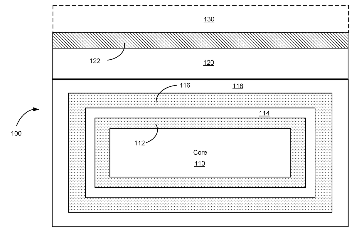
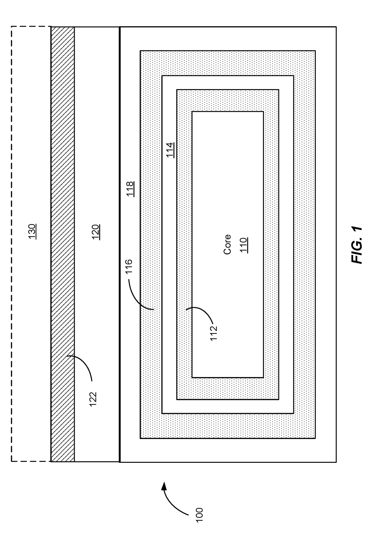
[0038]FIG. 1 is a simplified schematic cross-sectional diagram illustrating an engineered substrate structure according to an embodiment of the present invention. The engineered substrate 100 illustrated in FIG. 1 is suitable for a variety of electronic and optical applications. The engineered substrate 100 includes a core...


PUM

PropertyMeasurementUnit
thicknessaaaaaaaaaa
thicknessaaaaaaaaaa
thicknessaaaaaaaaaa

Abstract

A semiconductor diode includes an engineered substrate including a substantially single crystal layer, a buffer layer coupled to the substantially single crystal layer, and a semi-insulating layer coupled to the buffer layer. The semiconductor diode also includes a first N-type gallium nitride layer coupled to the semi-insulating layer and a second N-type gallium nitride layer coupled to the first N-type gallium nitride layer. The first N-type gallium nitride layer has a first doping concentration and the second N-type gallium nitride layer has a second doping concentration less than the first doping concentration. The semiconductor diode further includes a P-type gallium nitride layer coupled to the second N-type gallium nitride layer, an anode contact coupled to the P-type gallium nitride layer, and a cathode contact coupled to a portion of the first N-type gallium nitride layer.

Description

CROSS-REFERENCES TO RELATED APPLICATIONS[0001]This application claims priority to U.S. Provisional Patent Application No. 62 / 378,382, filed on Aug. 23, 2016, the disclosure of which is hereby incorporated by reference in its entirety for all purposes.[0002]The following regular U.S. patent applications (including this one) are being filed concurrently, and the entire disclosure of the other application is incorporated by reference into this application for all purposes:[0003]Application Ser. No. 15 / 684,724, filed Aug. 23, 2017, entitled “ELECTRONIC POWER DEVICES INTEGRATED WITH AN ENGINEERED SUBSTRATE” (Attorney Docket No. 098825-1059886-003311US); and[0004]Application Ser. No. ______, filed Aug. 23, 2017, entitled “VERTICAL SEMICONDUCTOR DIODE MANUFACTURED WITH AN ENGINEERED SUBSTRATE” (Attorney Docket No. 098825-1058838-003320US).BACKGROUND OF THE INVENTION[0005]Gallium nitride based power devices are typically epitaxially grown on sapphire substrates. The growth of gallium nitrid...

Claims


Application Information

Patent Timeline
Patent Type & Authority Applications(United States)
IPC IPC(8): H01L21/02H01L29/20H01L29/205H01L29/872H01L29/66H01L29/778C30B29/06C30B29/40C30B25/18
CPCH01L21/0242H01L29/2003H01L29/205H01L29/872H01L29/66143H01L29/7787H01L29/66462H01L21/02428H01L21/02458H01L21/0254H01L21/0257C30B29/06C30B29/406C30B25/183H01L29/402H01L29/7786H01L29/8613H01L29/1066H01L21/18H01L21/28587H01L29/4175H01L29/4236H01L29/66204H01L29/861H01L21/02505H01L27/105H01L27/0605H01L21/762H01L21/28264H01L21/4807H01L21/6835H01L29/1033H01L29/42376H01L2221/68345H01L2221/6835
Inventor ODNOBLYUDOV, VLADIMIRRISBUD, DILIPAKTAS, OZGURBASCERI, CEM
Owner QROMIS INC
Why Eureka
Try Eureka