Location-Specific Tuning of Stress to Control Bow to Control Overlay In Semiconductor Processing

a technology of stress and location, applied in the field of semiconductor fabrication, can solve the problems of overlay errors, expansion exceeds overlay error tolerances, and large overlay errors, and achieve the effect of reducing overlay errors

Active Publication Date: 2018-03-08
TOKYO ELECTRON LTD
View PDF1 Cites 19 Cited by
  • Summary
  • Abstract
  • Description
  • Claims
  • Application Information

AI Technical Summary

Benefits of technology

[0009]Techniques herein include a method for correcting wafer overlay. In one embodiment of this method, a substrate is received that has a working surface and that has a backside surface opposite to the working surface. The substrate has an initial overlay error resulting from one or more micro fabrication processing steps that have been executed to create at least part of a semiconductor device on the working surface of the substrate. An initial bow measurement of the substrate is received or taken that maps z-height deviations on the substrate relative to one or more reference z-height values. An overlay correction pattern is generated that defines adjustments to internal stresses at specific locations on the substrate based on the initial bow measurement of the substrate. In this overlay correction pattern, a first given location on the substrate has a different internal stress adjustment defined as compared to a second given location on the substrate in the overlay correction pattern. Internal stresses on the substrate are then modified at specific locations on the substrate according to the overlay correction pattern resulting in a modified bow of the substrate. The substrate with the modified bow has a second overlay error. The second overlay error has reduced overlay error as compared to the initial overlay error.

Problems solved by technology

An error in overlay means that a layer is offset with respect to a layer below (or above) it.
Any movement of the substrate relative to the substrate stage after alignment, however, can result in overlay errors.
If the substrate expansion is unchecked, the expansion exceeds overlay error tolerances.
Moreover, if the clamping force between the substrate and the substrate chuck is not sufficient to prevent substrate expansion, then the substrate can slip on the substrate chuck and larger substrate expansion will occur, resulting in larger overlay errors.
Thus, vacuum clamping is not always possible, and the weaker electrostatic clamping must be used in lieu of a vacuum clamp.
Other fabrication steps can also cause substrate expansion and contraction.
For example, deposited films can cause substrate contraction.
Also, various annealing and doping steps can create substantial amounts of bow in a given substrate.
Annealing steps can especially create overlay challenges.
The result of these various fabrication steps is a substrate that is uneven or non-planar.
Thus having deflection variations of thousands of nanometers to 10,000 nanometers can dramatically reduce yield as it is difficult to properly align two patterns.
With such significant bowing, however, it can be very difficult or impossible to accurately flatten a substrate by chucking a substrate alone.
The substrate has an initial overlay error resulting from one or more micro fabrication processing steps that have been executed to create at least part of a semiconductor device on the working surface of the substrate.

Method used


Image

  • Location-Specific Tuning of Stress to Control Bow to Control Overlay In Semiconductor Processing
  • Location-Specific Tuning of Stress to Control Bow to Control Overlay In Semiconductor Processing
  • Location-Specific Tuning of Stress to Control Bow to Control Overlay In Semiconductor Processing

Examples


Embodiment Construction

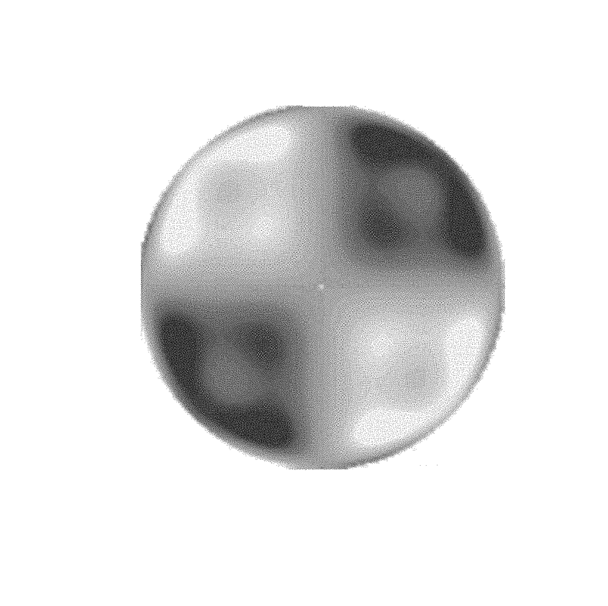
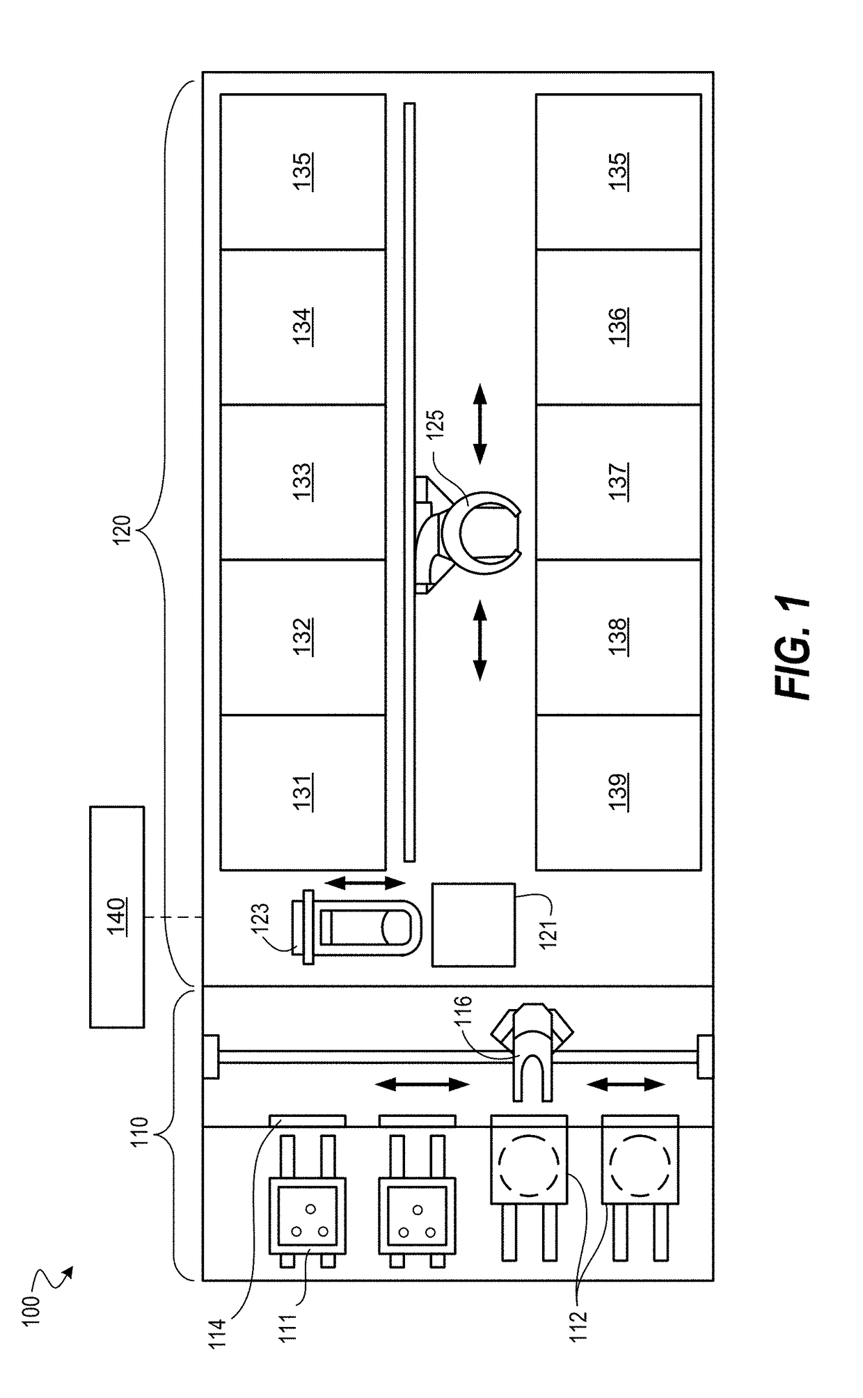
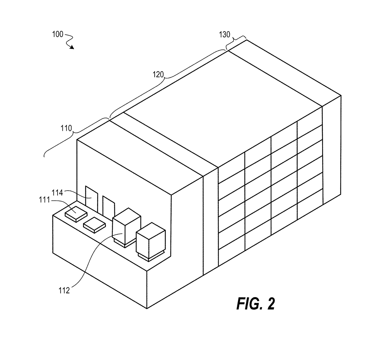
[0030]Techniques herein include systems and methods for correcting pattern overlay errors by correcting or adjusting bowing of semiconductor substrates (wafers). Techniques herein include systems and methods for location-specific tuning of stress on wafers to reduce overlay error. Location-specific tuning of stress independently modifies specific regions, areas, or point locations on a substrate to change wafer bow at those specific locations. Such spatial stress tuning with differential control reduces overlay error on substrates, which in turn improves overlay of subsequent patterns created on the substrate. Techniques herein include receiving a substrate with some amount of overlay error, measuring bow of the substrate to map z-height deviations across the substrate, generating an overlay correction pattern, and then physically modifying internal stresses on the substrate at specific locations with these modifications and intensities being independent of other locations. Such mod...


PUM

PropertyMeasurementUnit
height deviationaaaaaaaaaa
diameteraaaaaaaaaa
z-heightaaaaaaaaaa

Abstract

Techniques herein include systems and methods for correcting pattern overlay errors by correcting or adjusting bowing of wafers. Location-specific tuning of stress on semiconductor substrates reduces overlay error. Location-specific tuning of stress independently modifies specific regions, areas, or point locations on a substrate to change wafer bow at those specific locations, which reduces overlay error on substrates, which in turn improves overlay of subsequent patterns created on the substrate. Techniques herein include receiving a substrate with some amount of overlay error, measuring bow of the substrate to map z-height deviations across the substrate, generating an overlay correction pattern, and then physically modifying internal stresses on the substrate at specific locations with modifications independent of other coordinate locations. Such modifications can include etching a backside surface of the substrate. One or more processing modules can be used for such processing.

Description

CROSS REFERENCE TO RELATED APPLICATIONS[0001]The present application claims the benefit of U.S. Provisional Patent Application No. 62 / 383,549, filed on Sep. 5, 2016, entitled “Method for Correcting Wafer Bow,” which is incorporated herein by reference in its entirety.BACKGROUND OF THE INVENTION[0002]This disclosure relates to semiconductor fabrication, and particularly to wafer overlay.[0003]Semiconductor fabrication involves multiple varied steps and processes. One typical fabrication process is known as photolithography (also called microlithography). Photolithography uses radiation, such as ultraviolet or visible light, to generate fine patterns in a semiconductor device design. Many types of semiconductor devices, such as diodes, transistors, and integrated circuits, can be constructed using semiconductor fabrication techniques including photolithography, etching, film deposition, surface cleaning, metallization, and so forth.[0004]Exposure systems (also called tools) are used t...

Claims


Application Information

Patent Timeline
Patent Type & Authority Applications(United States)
IPC IPC(8): H01L21/302H01L21/66H01L21/027G03F7/20
CPCH01L21/302H01L22/20H01L22/12H01L22/30H01L21/027G03F7/70633H01L21/68G03F7/70783H01L21/0274H01L21/67115H01L21/6715H01L21/67288H01L21/6875G06F30/23H01L22/32H01L22/26H01L21/67259H01L21/67253G06F30/20G06T7/0004G06T2207/30148G03F7/70525
Inventor DEVILLIERS, ANTON J.FULFORD, DANIEL
Owner TOKYO ELECTRON LTD
Why Eureka
Try Eureka