Integrated circuits including a dummy metal feature and methods of forming the same

Active Publication Date: 2018-03-15
GLOBALFOUNDRIES SINGAPORE PTE LTD
View PDF2 Cites 0 Cited by
  • Summary
  • Abstract
  • Description
  • Claims
  • Application Information

AI Technical Summary

Benefits of technology

This patent describes a new method of making integrated circuits with a semiconductor substrate having an isolated well. A multilayer metallization stack is used to connect to the isolated well and includes a metal layer, a functional via, and a dummy metal feature. The technology allows for more efficient use of space and better performance of the integrated circuit.

Problems solved by technology

During formation of certain features in integrated circuits, such as NVM devices, electrical charges can build up and become trapped in isolated wells of the semiconductor substrate.
As a result, electrical charges can become trapped in the isolated p-wells.
As a result of forming the electrical circuit through the solvent, galvanic corrosion may occur in various metal features, especially in vias connecting to higher levels of metal layers where a significantly smaller number of vias are employed as compared to vias connecting to lower levels of metal layers.
The galvanic corrosion leads to metal void formation in the affected metal features, ultimately resulting in compromised function of the integrated circuits.
Additionally, galvanic corrosion is generally more prevalent in metal features that are in electrical communication with the isolated p-well.
However, such diodes are not suitable for certain devices that employ high voltages during intended usage.
Because tie-down diodes effectively release current upon exceeding the voltage threshold of the diodes, the maximum voltage that can be introduced into the isolated well is the voltage threshold of the tie-down diode and programming of the NVM devices would therefore not be possible with use of tie-down diodes.

Method used


Image

  • Integrated circuits including a dummy metal feature and methods of forming the same
  • Integrated circuits including a dummy metal feature and methods of forming the same
  • Integrated circuits including a dummy metal feature and methods of forming the same

Examples


Embodiment Construction

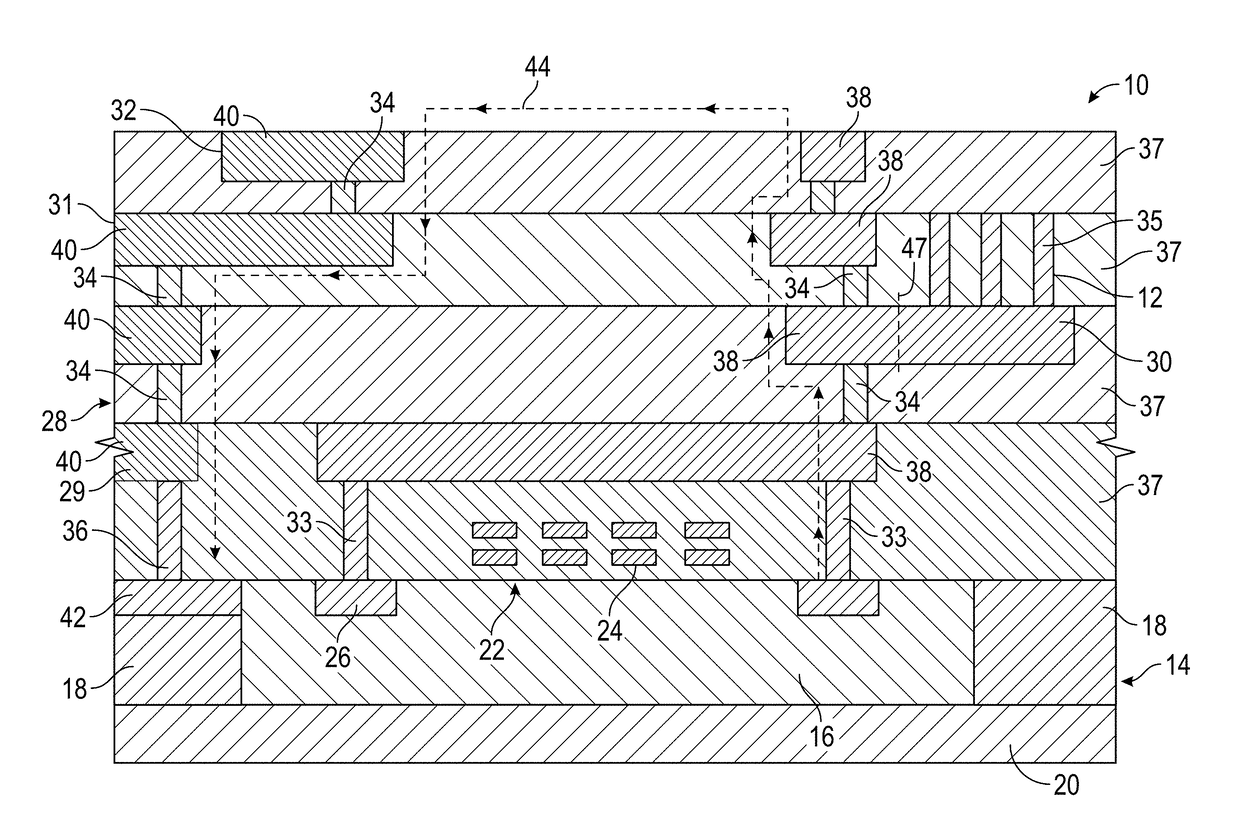
[0013]The following detailed description is merely exemplary in nature and is not intended to limit the integrated circuits and methods of forming the integrated circuits as set forth in the accompanying claims. Furthermore, there is no intention to be bound by any theory presented in the preceding background or the following detailed description.

[0014]Embodiments of the present disclosure are generally directed to integrated circuits and methods for fabricating the same. For the sake of brevity, conventional techniques related to integrated circuit device fabrication may not be described in detail herein. Moreover, the various tasks and process steps described herein may be incorporated into a more comprehensive procedure or process having additional steps or functionality not described in detail herein. In particular, various steps in the manufacture of semiconductor-based transistors are well-known and so, in the interest of brevity, many conventional steps will only be mentioned...


PUM


Abstract

Integrated circuits and methods of forming the same are provided herein. In an embodiment, an integrated circuit includes a semiconductor substrate that has an isolated well. A multilayer metallization stack overlies the semiconductor substrate. The multilayer metallization stack includes a metal layer, a functional via, and a dummy metal feature. The metal layer includes a first line in electrical communication with the isolated well through a contact. The functional via is in electrical communication with the first line and the contact. The dummy metal feature is in electrical communication with the functional via.

Description

TECHNICAL FIELD[0001]The technical field generally relates to integrated circuits that include a dummy metal feature and methods of forming the same. More particularly, the technical field relates to integrated circuits that include a dummy metal feature to minimize galvanic corrosion and metal void formation in other metal features during fabrication of the integrated circuit.BACKGROUND[0002]The majority of present day integrated circuits (ICs) are implemented by using a plurality of interconnected field effect transistors (FETs), also called metal oxide semiconductor field effect transistors (MOSFETs or MOS transistors). A MOS transistor includes a gate electrode as a control electrode overlying a well in a semiconductor substrate and spaced-apart source and drain regions in the well between which a current can flow. In addition to MOS transistors, ICs often contain various additional devices such as, e.g., non-volatile memory (NVM) devices.[0003]During formation of certain featur...

Claims


Application Information

Patent Timeline
IPC IPC(8): H01L23/522H01L23/528H01L27/115H01L21/768
CPCH01L23/5225H01L23/5226H01L21/76877H01L27/115H01L21/76816H01L23/528H01L23/522H10B41/40H10B69/00
Inventor SHENG, HAIFENGZHAO, SHIFENGTAN, JUAN BOONSIAH, SOH YUN
Owner GLOBALFOUNDRIES SINGAPORE PTE LTD
Why Eureka
Try Eureka