
Transient voltage suppressor and method for manufacturing the same

a transient voltage suppressor and manufacturing method technology, applied in the direction of emergency protective circuit arrangement, transistor, etc., can solve the problems of increasing the need for transient voltage suppressors, affecting and devices including integrated circuits easily damaged, so as to achieve the effect of improving the robustness of transient voltage suppressors without increasing the manufacture cos

Active Publication Date: 2018-03-29
SILERGY SEMICON TECH (HANGZHOU) CO LTD
View PDF1 Cites 13 Cited by
  • Summary
  • Abstract
  • Description
  • Claims
  • Application Information

AI Technical Summary

Benefits of technology

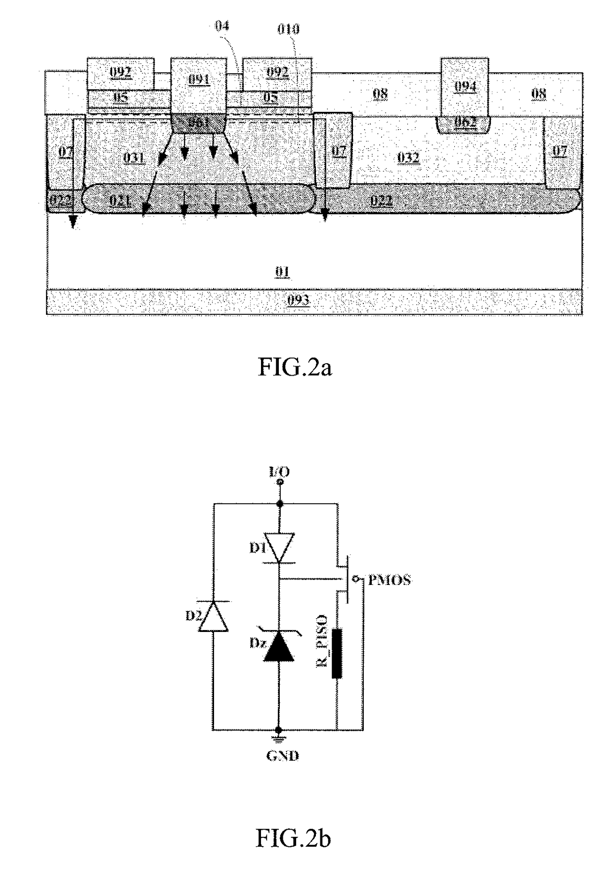
This patent provides a transient voltage suppressor (TVS) with better resistance to damage from large currents, while also reducing parasitic capacitance. The method includes adding an additional gate stack layer and reusing diffusion isolation regions as conductive vias. When there is a large current, a MOS transistor is turned on to protect the TVS from damage. This makes the TVS more robust without increasing manufacturing costs.

Problems solved by technology

As the quantity of the devices including the integrated circuits easily damaged by over-voltages increases, the need for transient voltage suppressors also increases.
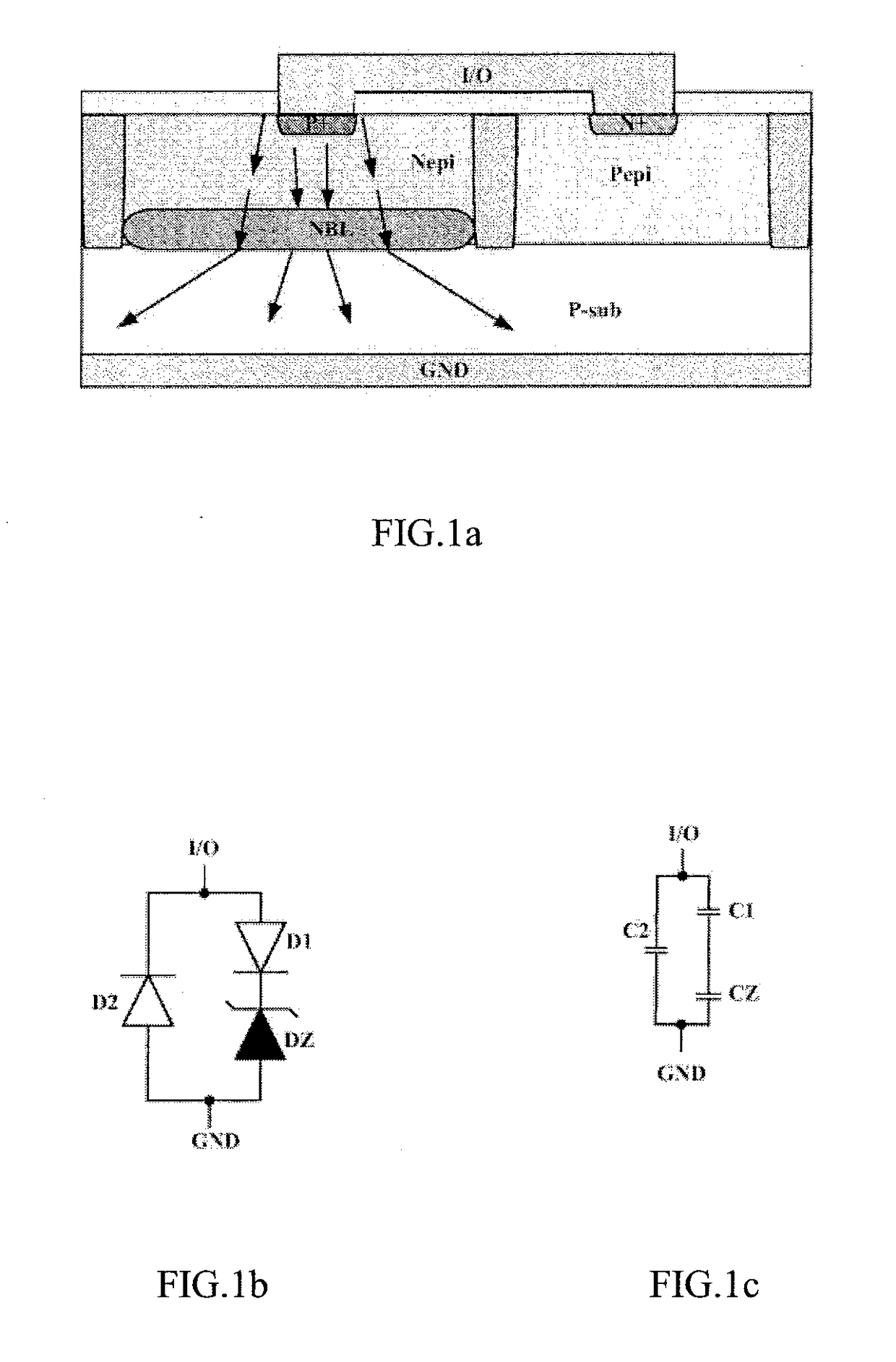
However, if the junction area of the diode D1 is designed to be small, the robustness of the transient voltage suppressor will be affected, that means, the transient voltage suppressor cannot withstand a large surge current or a large electrostatic current.
Therefore, the prior transient voltage suppressor cannot implement better robustness as obtaining a low capacitance value.

Method used


Image

  • Transient voltage suppressor and method for manufacturing the same
  • Transient voltage suppressor and method for manufacturing the same
  • Transient voltage suppressor and method for manufacturing the same

Examples


Embodiment Construction

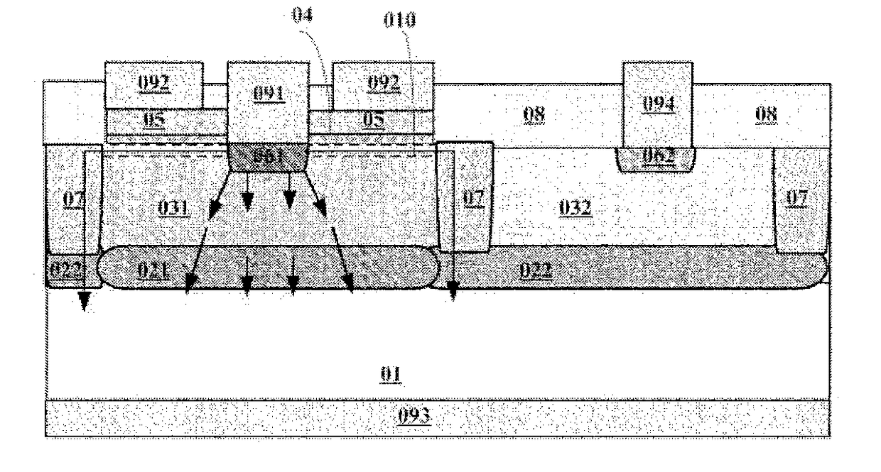
[0066]Exemplary embodiments of the present disclosure will be described in more details below with reference to the accompanying drawings. In the drawings, like reference numerals denote like members. The figures are not drawn to scale, for the sake of clarity. Moreover, some well-known parts may not be shown. For simplicity, the structure having been subject to several relevant process steps may be shown in one figure. Some particular details of the present disclosure will be described below, such as exemplary semiconductor structures, materials, dimensions, process steps and technologies of the members, for better understanding of the present disclosure. However, it can be understood by one skilled person in the art that these details are not always essential but can be varied in a specific implementation of the disclosure.

[0067]FIG. 2a is a structural diagram of a transient voltage suppressor according to an embodiment of the disclosure and FIG. 2b is an equivalent circuit diagra...


PUM


Abstract

Disclosed a transient voltage suppressor and a method for manufacturing the same. According to the transient voltage suppressor, an additional gate stack layer is introduced based on the prior transient voltage suppressor, and the diffusion isolation regions are reused as the conductive vias, so that, the gate stack layer, the first doped region, the conductive vias, and the second semiconductor layer constitute a MOS transistor being coupled in parallel to the Zener diode or the avalanche diode of the transient voltage suppressor. When the current of the I / O terminal is relatively large, the MOS transistor is turned on to share part of the current of the I / O terminal through the Zener diode or the avalanche diode, thereby protecting the Zener diode or the avalanche diode from being damaged due to excessive current. Thus, the robustness of the transient voltage suppressor is improved without increasing the manufacture cost.

Description

CROSS-REFERENCE TO RELATED APPLICATION[0001]This application claims the benefit of Chinese Patent Application No. 201610845693.3, filed on Sep. 23, 2016, which are incorporated herein by reference in its entirety.BACKGROUND OF THE DISCLOSUREField of the Disclosure[0002]The present disclosure relates to a semiconductor device and a method for manufacturing the same, and in particular, to a transient voltage suppressor and a method for manufacturing the same.Background of the Disclosure[0003]Transient voltage suppressors (TVS) are used to protect integrated circuits from being damaged by over-voltages suddenly occurred on the integrated circuits. As the quantity of the devices including the integrated circuits easily damaged by over-voltages increases, the need for transient voltage suppressors also increases. For example, USB power supplies, data line protectors, video interfaces, high-speed Ethernet devices, laptops, monitors, flat panel displays and so on are all need to employ tra...

Claims


Application Information

Patent Timeline
Patent Type & Authority Applications(United States)
IPC IPC(8): H01L27/02H02H9/04H01L21/02
CPCH01L27/0248H02H9/04H01L21/02697H01L21/02293H01L27/0266H01L27/0255H01L29/861H01L29/402
Inventor YIN, DENGPINGWANG, SHIJUNYAO, FEI
Owner SILERGY SEMICON TECH (HANGZHOU) CO LTD
Learn More