Linearized negative impedance converter matching circuits and impedance adjustment circuit for a negative impedance converter

a negative impedance converter and matching circuit technology, applied in the direction of impedence converters, multiple-port active networks, impedence matching networks, etc., can solve the problems of reducing antenna efficiency, reducing total efficiency, and reducing antenna radiation resistance, so as to improve in-band matching performance and improve total efficiency and return loss, avoid excessive negative resistance, the effect of strengthening the adjustment

Inactive Publication Date: 2018-05-03
SMART ANTENNA TECH
View PDF0 Cites 7 Cited by
  • Summary
  • Abstract
  • Description
  • Claims
  • Application Information

AI Technical Summary

Benefits of technology

[0032]The second diode or further transistor helps to compensate for voltage changes in the first diode or third transistor due to physical environmental changes, such as temperature.
[0052]In certain embodiments, the capacitor(s) in the passive impedance network may be a simple fixed capacitor(s), with a capacitance selected to be the same value as the combined parasitic capacitances in the transistors of the NIC. Accordingly, there is no need for expensive varactors or variable capacitors.

Problems solved by technology

However, the resistive loss that is introduced by the inductor Lext dramatically degrades the total efficiency.
The reduction in size means that the antenna radiation resistance also reduces, and this in turn leads to a reduction the antenna efficiency.
These two fundamental limits on the antenna make it difficult to provide a small antenna with a low Q (wideband).
However, more and more devices these days require smaller antennas and there is need for these antennas to still have wide usable bandwidths.
Passive matching networks help to match antennas, but because they involve resonating the reactive part of the antenna with passive elements, they only give a good match at specific frequencies.
This will work, but the amount of battery power consumed at lower transmit powers in a handset, tablet or other mobile device is wasteful.
This may satisfy the linearity requirement at maximum transmitter power (24 dBm for LTE), but for lower transmit powers this is clearly wasteful.
However, in both of these NIC devices, bias is applied to both the base of one transistor and to the collector of the other transistor.
However, the present Applicant has found that conventional Linvill-type NIC matching circuits as shown in FIG. 9 are not always ideal enough to generate the precise negative impedance that is required in particular antenna applications.
This can result in lower total efficiency, higher noise figures and potential instability.

Method used


Image

  • Linearized negative impedance converter matching circuits and impedance adjustment circuit for a negative impedance converter
  • Linearized negative impedance converter matching circuits and impedance adjustment circuit for a negative impedance converter
  • Linearized negative impedance converter matching circuits and impedance adjustment circuit for a negative impedance converter

Examples


Embodiment Construction

[0076]FIG. 10 illustrates an embodiment comprising an NIC-based matching circuit for an electrically small antenna. The circuit comprises an output termination 1, a two-port antenna model 2, a neutralization inductor 3, an NIC block 4, a capacitor 5 for impedance transformation and an RF source 6.

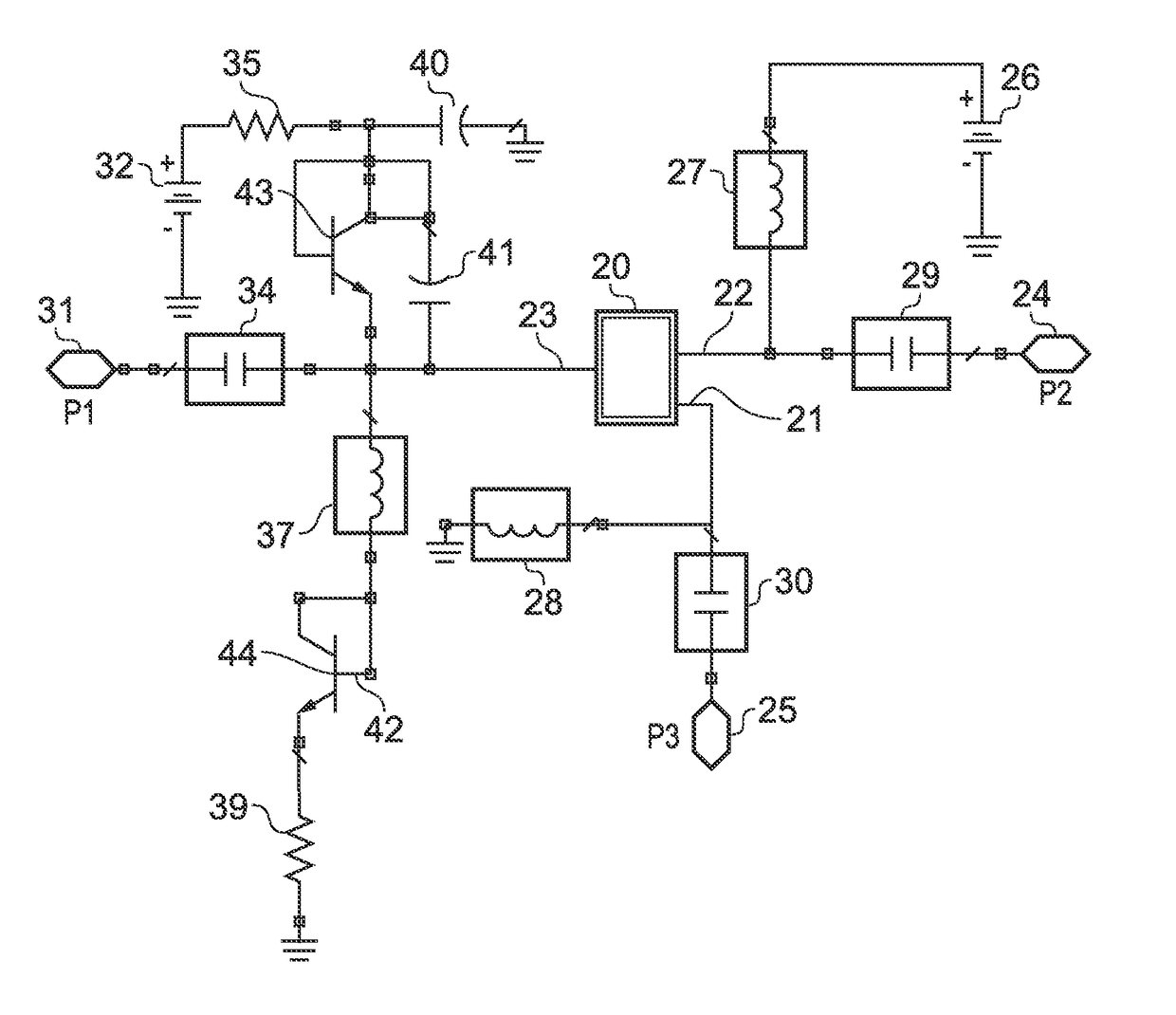
[0077]FIG. 11 shows the NIC block 4 in more detail, the NIC including an input port 7 connected to the emitter or source port P3 of a first transistor sub-circuit 9, and an output port 8 connected to the emitter or source port P3 of a second transistor sub-circuit 10. The transistor sub-circuits 9, 10 are connected in a cross-over configuration, with the base or gate port P1 of the first transistor sub-circuit 9 connected to the collector or drain port P2 of the second transistor sub-circuit 10, and the collector or drain port P2 of the first transistor sub-circuit 9 connected to the base or gate port P1 of the second transistor sub-circuit 10. A capacitor 100 and a lossy inductor 101 are c...


PUM


Abstract

There is disclosed a negative impedance converter for a matching circuit for matching an impedance of an antenna to an impedance of an RF source or load. The negative impedance converter comprises first and second transistors connected in a cross-over configuration. Each transistor has a source or emitter, a drain or collector and a gate or base, and each transistor further has a first biasing circuit connected to its gate or base. The first biasing circuit comprises a first DC biasing signal source and a first diode or a third transistor connected between the first DC biasing signal source and the gate or base. There is also disclosed a negative impedance converter for a matching circuit for matching an impedance of an antenna to an impedance of an RF source or load. The negative impedance converter comprises first and second transistors connected in a cross-over configuration, each transistor having a source or emitter, a drain or collector and a gate or base. The source or emitter of one transistor is configured as an RF input port and the source or emitter of the other transistor is configured as an RF output port. The drain or collector of the first transistor is connected to the gate or base of the second transistor and the drain or collector of the second transistor is connected to the gate or base of the first transistor. An impedance is connected between the drain or collector of the first transistor and the drain or collector of the second transistor. The negative impedance converter is further provided with a passive impedance adjustment network connected between the source or emitter of the first transistor and the source or emitter of the second transistor.

Description

[0001]This invention relates to matching circuits to match antennas to RF sources and, in particular, to matching circuits comprising a negative impedance converter provided with bias circuitry configured to improve linearity performance. In other aspects, this invention relates to matching circuits to match antennas to RF sources and, in particular, to an impedance adjustment circuit for a negative impedance converter implemented in a matching circuit.BACKGROUND[0002]Electrically small antennas can be generally classified as TM (transverse magnetic) and TE (transverse electric) mode antennas. For a TM mode small antenna, which is widely used in wireless communication systems, the input impedance is considerably reactive with a small real part. It is therefore critical to match the antenna to the receiver or transmitter to maximise the total efficiency in the frequency range of interest.[0003]Normally, an electrically small TM mode antenna can be characterised by or represented as a...

Claims


Application Information

Patent Timeline
Patent Type & Authority Applications(United States)
IPC IPC(8): H03H11/30H03H11/44
CPCH03H11/30H03H11/44H03H11/28
Inventor HU, SAMPSONWAN, LIANG
Owner SMART ANTENNA TECH
Why Eureka
Try Eureka