Silicon ingot slicing apparatus using microbubbles and wire electric discharge machining

a technology of ingot slicing and microbubbles, which is applied in the direction of metal-working machine components, manufacturing tools, and working accessories, etc., can solve the problems of increasing kerf loss, increasing kerf loss, and surface defects, and achieve the effect of improving the quality of the sliced surfa

Active Publication Date: 2018-05-17
KOREA INST OF ENERGY RES
View PDF6 Cites 3 Cited by
  • Summary
  • Abstract
  • Description
  • Claims
  • Application Information

AI Technical Summary

Benefits of technology

[0007]It is an object of the present invention to provide a silicon ingot slicing apparatus which reduces an applied voltage to 10...

Problems solved by technology

Since the frictional force generated at the mechanical method may cause various defects on the surface of the silicon ingot, it is necessary to remove additional surface defects by using mechanical surface abrasion such as grinding, lapping, and polishing, and chemical surface abrasion such as etching and cleaning.
However, due to the high electric resistance of silicon, the voltage required for slicing the silicon ingot is a high voltage of 100 V to 500 V, and thus thermal damage may be caused on the surface of the silicon ingot by the high-temperature melting heat generated at the time of slicing the silicon ingot.
In addition, when slicing silicon ingots...

Method used


Image

  • Silicon ingot slicing apparatus using microbubbles and wire electric discharge machining
  • Silicon ingot slicing apparatus using microbubbles and wire electric discharge machining
  • Silicon ingot slicing apparatus using microbubbles and wire electric discharge machining

Examples


Embodiment Construction

[0042]The advantages and features of the present invention and the method of achieving the advantages and features will become apparent with reference to the embodiments described in detail below with reference to the accompanying drawings. The present invention may, however, be embodied in many different forms and should not be construed as limited to the embodiments set forth herein. Rather, these embodiments are provided so that this disclosure will be thorough and complete, and will be provided to fully convey the scope of the invention to those skilled in the art, and the invention is defined only by the scope of the claims. Like reference numerals refer to like elements throughout the specification.

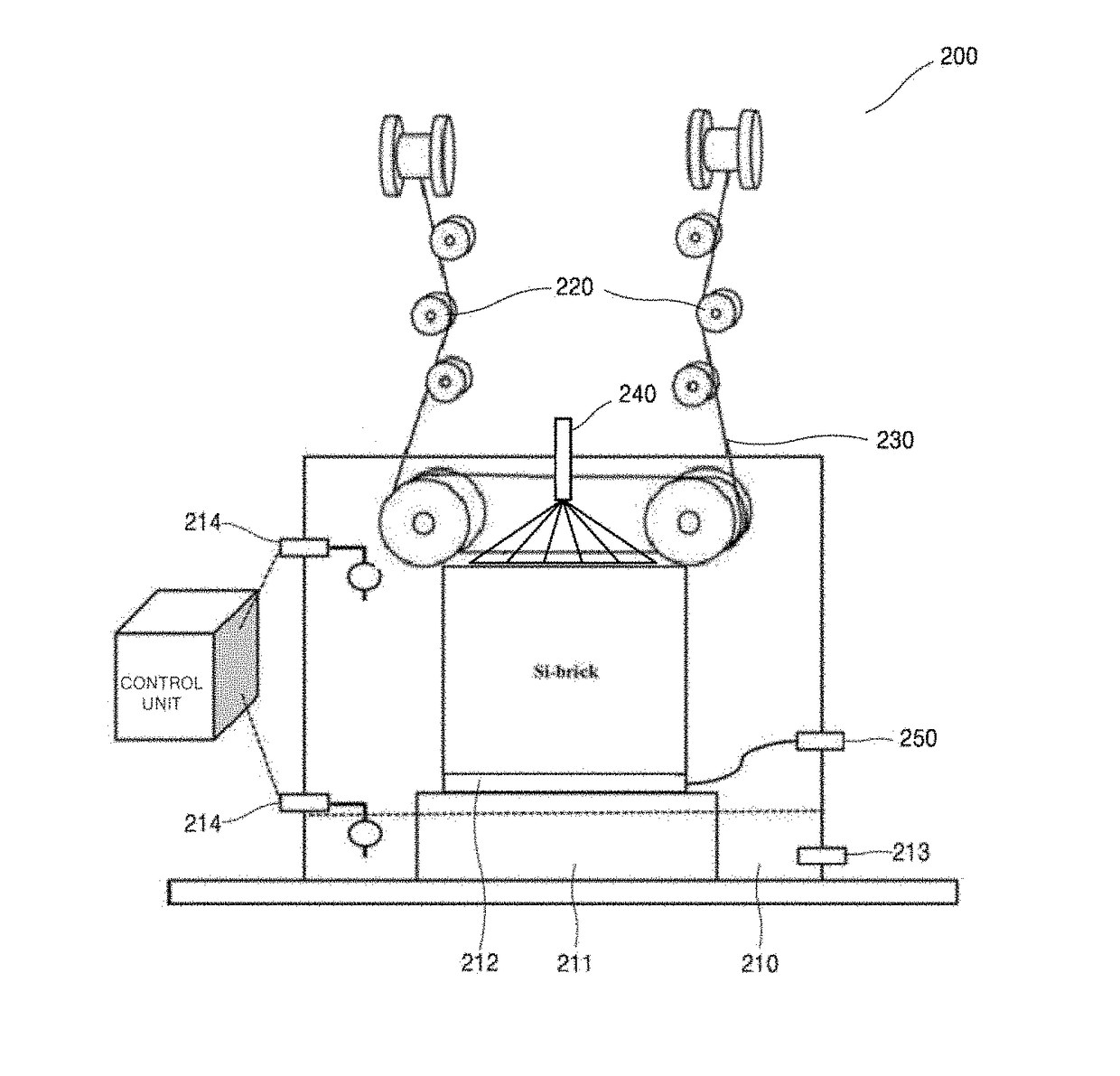
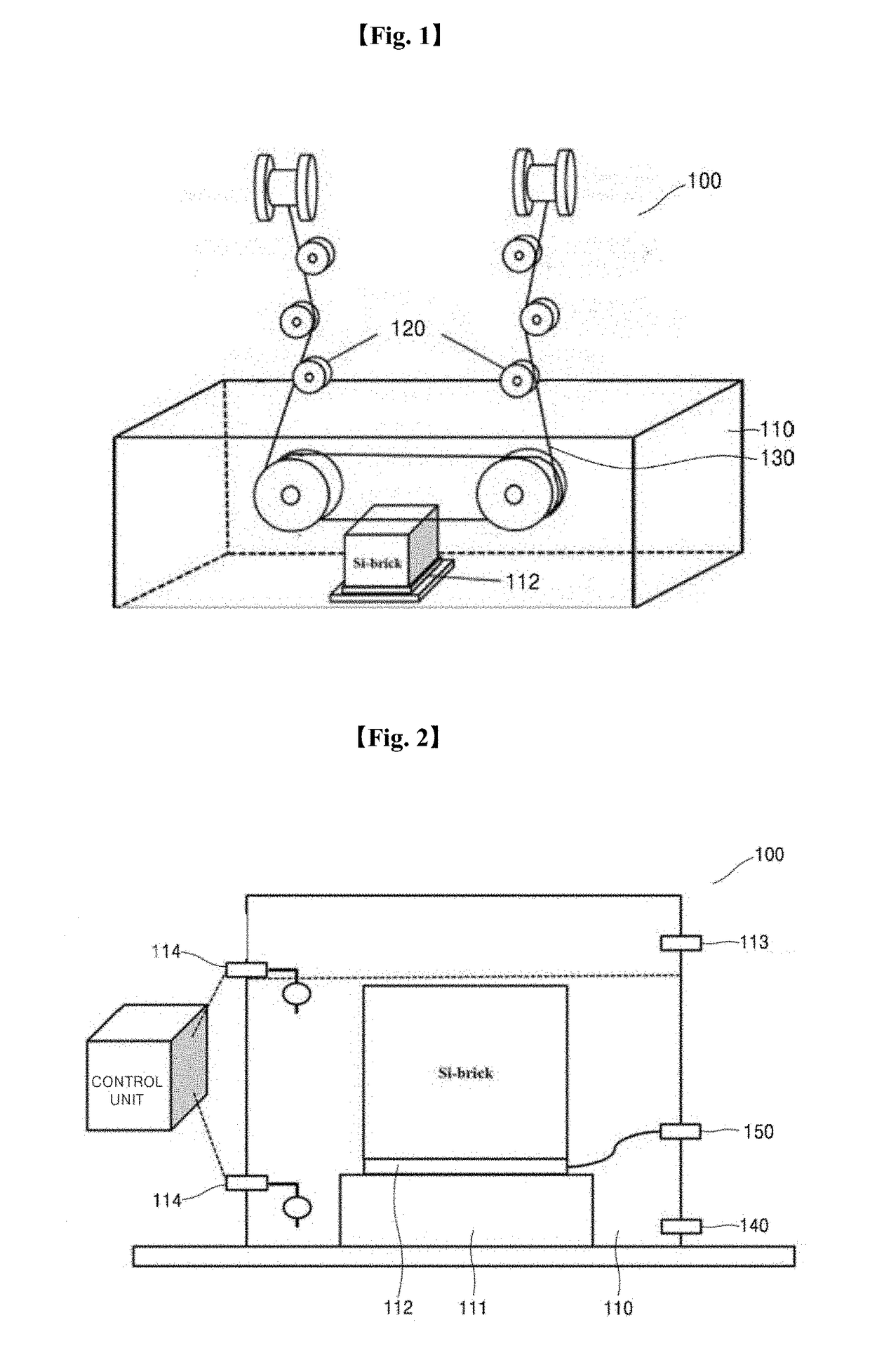
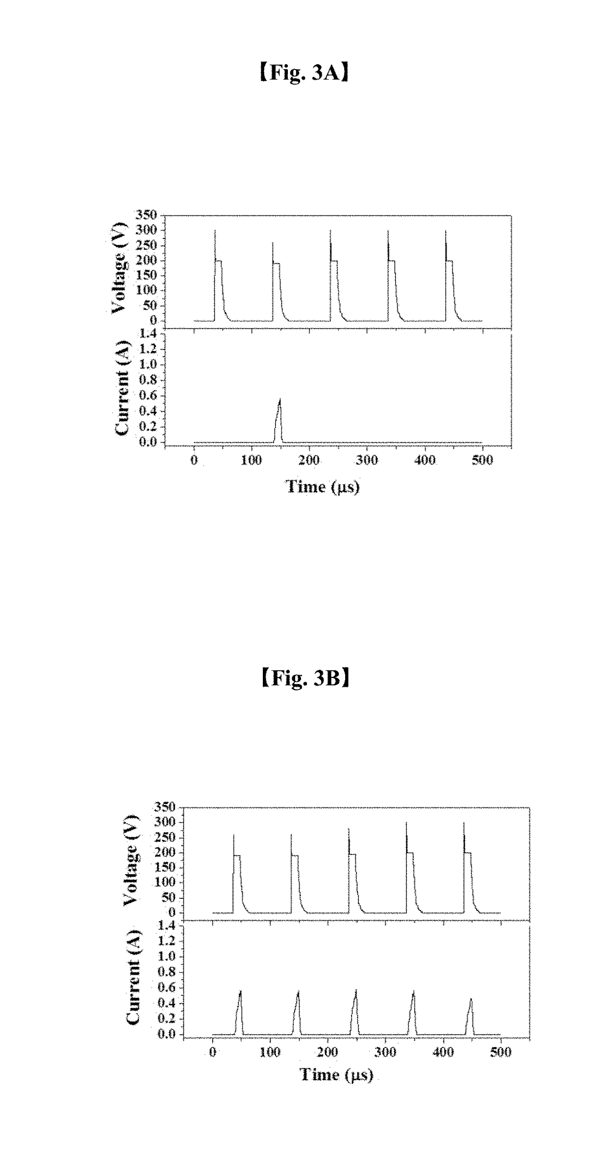
[0043]Hereinafter, a silicon ingot slicing apparatus using microbubbles and wire electric discharge machining according to a preferred embodiment of the present invention and a silicon ingot slicing method thereof will be described in detail with reference to the accompanying drawin...


PUM

PropertyMeasurementUnit
Electric potential / voltageaaaaaaaaaa
Particle diameteraaaaaaaaaa

Abstract

Provided are a silicon ingot slicing apparatus capable of slicing silicon ingots in various forms such as blocks or wafers using microbubbles and wire electric discharge machining.

Description

CROSS-REFERENCE TO RELATED APPLICATIONS[0001]This application claims priority to Korean Patent Application No. 10-2016-0151719 filed on Nov. 15, 2016, and Provisional Application No. 62 / 438,043 filed on Dec. 22, 2016, all the benefits accruing there from under 35 U.S.C. §119, the contents of which is incorporated by reference in its entirety.BACKGROUND1. Field of the Invention[0002]The present invention relates to a silicon ingot slicing apparatus and more particularly, to a silicon ingot slicing apparatus capable of slicing silicon ingots in various forms such as blocks or wafers using microbubbles and wire electric discharge machining, and a silicon ingot slicing method thereof.2. Description of the Related Art[0003]A method of slicing a silicon ingot by using a wire employs a mechanical method of rubbing a polishing slurry or a diamond coated wire against a silicon ingot, to thus slice the silicon ingot. Since the frictional force generated at the mechanical method may cause vari...

Claims


Application Information

Patent Timeline
IPC IPC(8): B28D5/04B28D5/00B26D7/27B23Q11/14B23Q11/12B26D3/28
CPCB28D5/045B28D5/0058B26D7/27C10N2240/06B23Q11/122B26D3/28C10N2240/401B23Q11/145B23H1/08B23H7/02B23H7/38B23H9/00B28D7/00H01L21/02002H01L21/67057H01L21/78C10N2040/06C10N2040/22
Inventor JANG, BO-YUNKIM, JOON-SOOMOON, HUI-CHANCHOI, SUN-HO
Owner KOREA INST OF ENERGY RES
Why Eureka
Try Eureka