Resistive environmental sensor and resistive environmental sensor array
- Summary
- Abstract
- Description
- Claims
- Application Information
AI Technical Summary
Benefits of technology
Problems solved by technology
Method used
Image

Examples
first embodiment
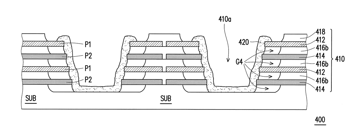
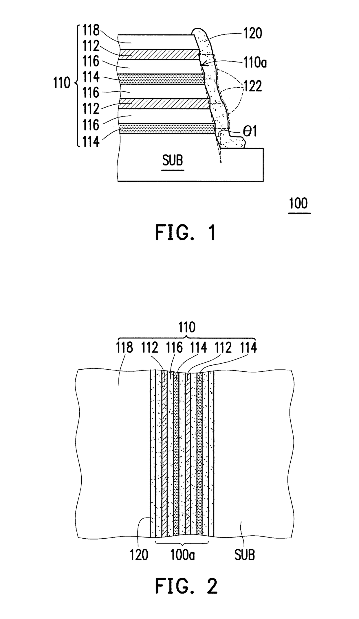
[0025]FIG. 1 and FIG. 3 are schematic cross-sectional views of a resistive environmental sensor according to a first embodiment of the invention, and FIG. 2 is a schematic top view of a first electrode layer, a second electrode layer, a dielectric layer, and a sensing layer in FIG. 1.
[0026]Referring to FIG. 1 and FIG. 2, a resistive environmental sensor 100 of the embodiment includes an electrode stack 110 and a sensing layer 120. The electrode stack 110 includes at least one first electrode layer 112, at least one second electrode layer 114, and at least one dielectric layer 116 disposed between the first electrode layer 112 and the second electrode layer 114, wherein the electrode stack 110 has a side surface 110a, and the first electrode layer 112 and the second electrode layer 114 are exposed on the side surface 110a of the electrode stack 110. The sensing layer 120 is disposed on the side surface 110a of the electrode stack 110, and the sensing layer 120 is in contact with the ...
second embodiment
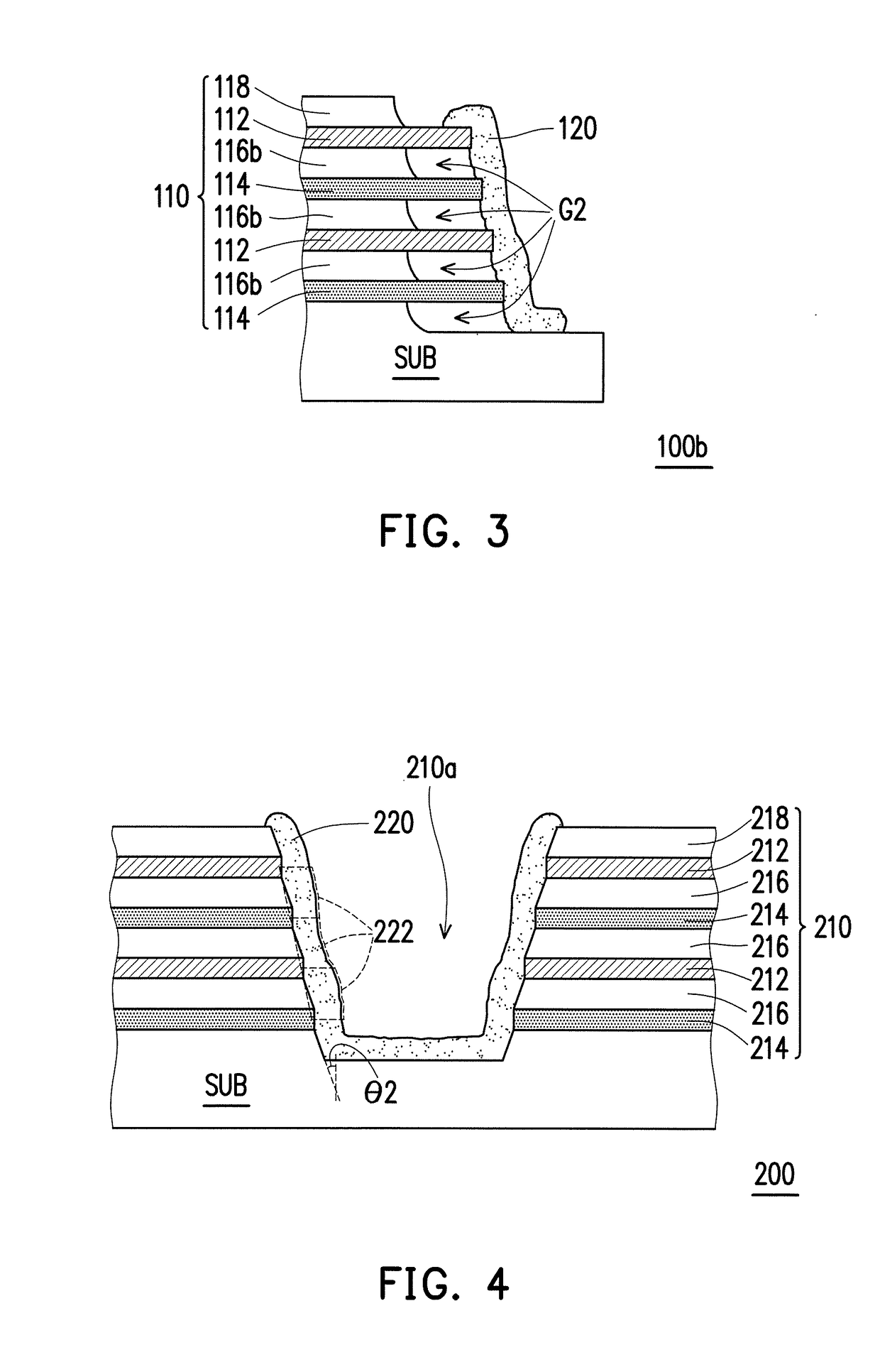
[0036]FIG. 4 and FIG. 6 are schematic cross-sectional views of a resistive environmental sensor according to a second embodiment of the invention, and FIG. 5 is a schematic top view of a first electrode layer, a second electrode layer, a dielectric layer, and a sensing layer in FIG. 4.
[0037]Referring to FIG. 4 and FIG. 5, a resistive environmental sensor 200 of the embodiment includes a circuit board 210 and a sensing layer 220. The circuit board 210 includes at least one first electrode layer 212, at least one second electrode layer 214, and at least one dielectric layer 216 disposed between the first electrode layer 212 and the second electrode layer 214, wherein the circuit board 210 has at least one groove 210a, so as to expose the first electrode layer 212 and the second electrode layer 214. The sensing layer 220 is disposed in the groove 210a, and the sensing layer 220 is in contact with the first electrode layer 212 and the second electrode layer 214. In the embodiment, detai...
third embodiment
[0048]FIG. 7 and FIG. 9 are schematic cross-sectional views of a resistive environmental sensor according to a third embodiment of the invention, and FIG. 8 is a schematic top view of a first electrode layer, a second electrode layer, a dielectric layer, and a sensing layer in FIG. 7.
[0049]Referring to FIG. 1 and FIG. 7 to FIG. 9 at the same time, resistive environmental sensors 300 and 300b of the embodiment are similar to the resistive environmental sensors 100 and 100b of the first embodiment respectively, and the main difference is that, the electrode stack 110 in the resistive environmental sensors 300 and 300b is an island structure protruding from the substrate SUB, and a sensing layer 120a covers a top surface 110b and the entire side surface 110a of the electrode stack 110.
[0050]In the embodiment, the electrode stack 110 has a bottom surface or a top surface with a shape of a square, a rectangle, a polygon, a circle, or an ellipsoid, for example. The electrode stack 110 is ...
PUM
 Abstract
Description
Claims
Application Information
 - Generate Ideas
- Intellectual Property
- Life Sciences
- Materials
- Tech Scout
- Unparalleled Data Quality
- Higher Quality Content
- 60% Fewer Hallucinations
Browse by: Latest US Patents, China's latest patents, Technical Efficacy Thesaurus, Application Domain, Technology Topic, Popular Technical Reports.
© 2025 PatSnap. All rights reserved.Legal|Privacy policy|Modern Slavery Act Transparency Statement|Sitemap|About US| Contact US: help@patsnap.com