Liquid crystal diffractive devices with nano-scale pattern and methods of manufacturing the same

a liquid crystal diffractive device and nano-scale technology, applied in the field of optical devices, to achieve the effect of progressively decreasing the width of the zon

Active Publication Date: 2018-05-24
MAGIC LEAP
View PDF0 Cites 58 Cited by
  • Summary
  • Abstract
  • Description
  • Claims
  • Application Information

AI Technical Summary

Benefits of technology

[0028]An innovative aspect of the subject matter of this application is implemented in a liquid crystal lens. The liquid crystal lens comprises a patterned substrate comprising at least a first zone comprising a first plurality of features oriented along a first direction and a second zone comprising a second plurality of features oriented along a second direction. The first plurality of features and the second plurality of features have a dimension less than or equal to about 100 nm. The lens comprises a liquid crystal layer over the patterned substrate, wherein molecules of the liquid crystal layer are self-aligned to the first and the second plurality of features. The dimension can comprise a length, a height, a depth or a width of the feature. The liquid crystal can comprise a polymerizable liquid crystal.
[0029]The patterned substrate can comprise a substrate having a layer disposed thereon that is patterned. The first and the second zones can comprise concentric ring-shaped zones. The lens can comprise between about 3 and 30 zones. For example, the lens can comprise at least five zones. A width of the zones can progressively decrease with distance from a center of the patterned substrate. In vari

Problems solved by technology

Because the human visual perception system is complex, it is challenging to produce an AR technology that facilitates a com

Method used


Image

  • Liquid crystal diffractive devices with nano-scale pattern and methods of manufacturing the same
  • Liquid crystal diffractive devices with nano-scale pattern and methods of manufacturing the same
  • Liquid crystal diffractive devices with nano-scale pattern and methods of manufacturing the same

Examples


example method

of Manufacturing a Liquid Crystal Device

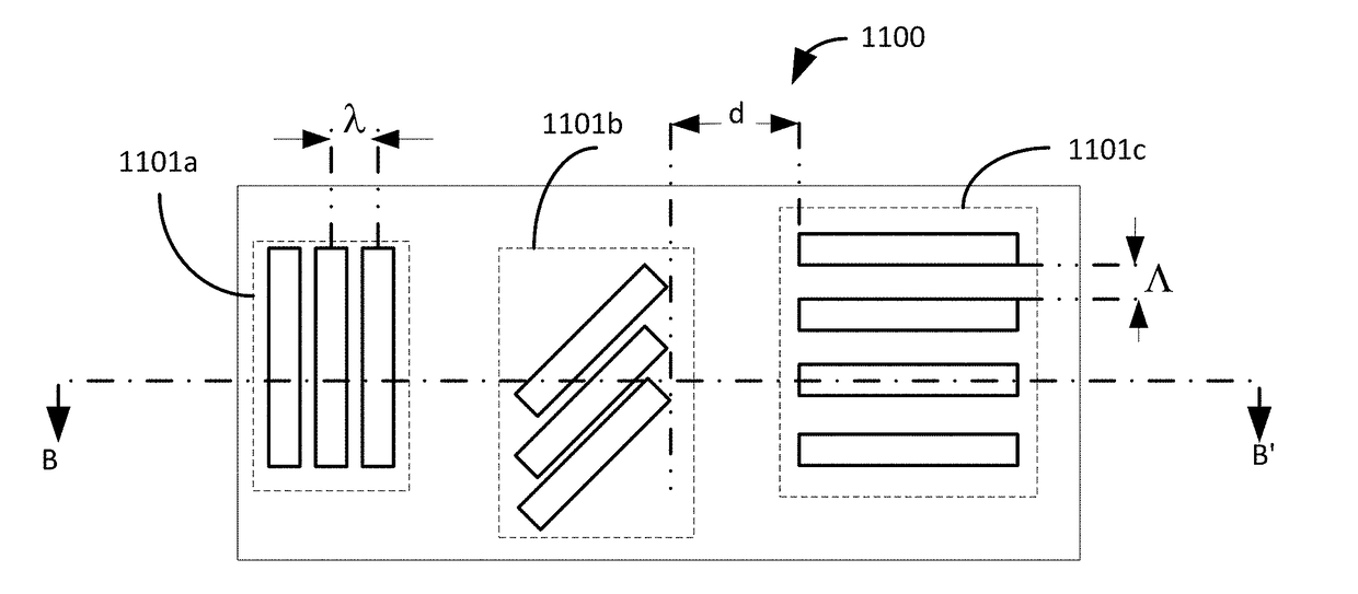
[0123]FIGS. 12A-12D illustrates an example of a method of manufacturing various liquid crystal devices described herein. Referring to FIG. 12A, a polymer liquid crystal (PLC) layer 1203 is disposed over a substrate 1201. The substrate 1201 is preferably optically transmissive. Examples of suitable materials for the substrate 1201 include glass, quartz, sapphire, indium tin oxide (ITO), or polymeric materials, including polycarbonate, polyacetate, and acrylic. In some embodiments, the substrate 1201 can be transmissive to light of at least one of visible wavelengths or infrared wavelengths. The substrate can include a pair of major surfaces and surrounding edges. The major surface may be the largest area surface of the substrate, or may be one of a pair of similarly-sized opposing surfaces each having larger areas than other surfaces. The liquid crystal devices can be configured to reflect, refract, diffract or otherwise redirect light incident...


PUM


Abstract

An optical device includes a liquid crystal layer having a first plurality of liquid crystal molecules arranged in a first pattern and a second plurality of liquid crystal molecules arranged in a second pattern. The first and the second pattern are separated from each other by a distance of about 20 nm and about 100 nm along a longitudinal or a transverse axis of the liquid crystal layer. The first and the second plurality of liquid crystal molecules are configured as first and second grating structures that can redirect light of visible or infrared wavelengths.

Description

PRIORITY CLAIM[0001]This application claims the priority benefit of U.S. Provisional Patent Application No. 62 / 424,341 filed on Nov. 18, 2016, which is incorporated by reference herein in its entiretyINCORPORATION BY REFERENCE[0002]This application incorporates by reference the entirety of each of the following patent applications: U.S. application Ser. No. 14 / 555,585 filed on Nov. 27, 2014; U.S. application Ser. No. 14 / 690,401 filed on Apr. 18, 2015; U.S. application Ser. No. 14 / 212,961 filed on Mar. 14, 2014; U.S. application Ser. No. 14 / 331,218 filed on Jul. 14, 2014; and U.S. application Ser. No. 15 / 072,290 filed on Mar. 16, 2016.BACKGROUNDField[0003]The present disclosure relates to optical devices, including virtual reality and augmented reality imaging and visualization systems.Description of the Related Art[0004]Modern computing and display technologies have facilitated the development of systems for so called “virtual reality” or “augmented reality” experiences, wherein dig...

Claims


Application Information

Patent Timeline
IPC IPC(8): G02F1/1347
CPCG02F1/1347B82Y20/00G02F2203/28G02F2203/24G02F1/133726G02B27/0081G02B27/0093G02B27/1006G02B3/00G02B30/36G02B5/1809G02B5/1833G02B5/1847G02B5/1861G02B5/3016G02B5/3083G02B6/00G02F1/29B81C1/0046G02B2006/0098G02B2027/0134G02B2027/0174G02B2027/0185
Inventor OH, CHULWOOMELLI, MAUROPEROZ, CHRISTOPHESINGH, VIKRAMJITXU, FRANKKLUG, MICHAEL ANTHONY
Owner MAGIC LEAP
Why Eureka
Try Eureka