Parallel Stacked Inductor for High-Q and High Current Handling and Method of Making the Same
a technology of parallel stacked inductor and high current, which is applied in the manufacture of coils, basic electric elements, inductances, etc., can solve the problems of parasitic effects that overwhelm the character of passive devices, the shape of the structure of microelectronic inductor is often limited to the availability of fabrication processes, etc., to achieve high quality factor (q factor), small size, and large inductance
- Summary
- Abstract
- Description
- Claims
- Application Information
AI Technical Summary
Benefits of technology
Problems solved by technology
Method used
Image

Examples
Embodiment Construction
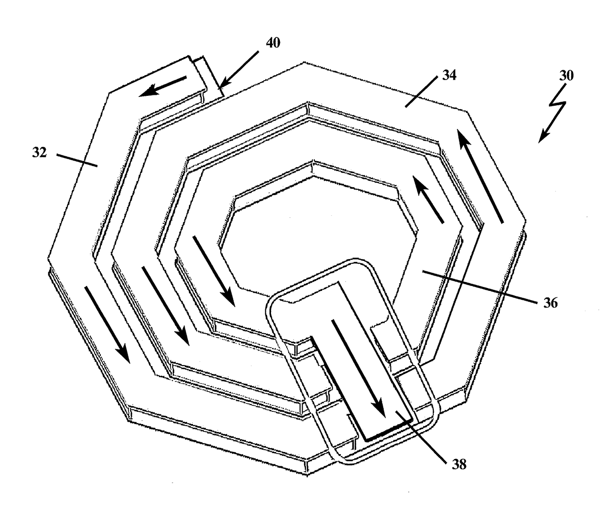
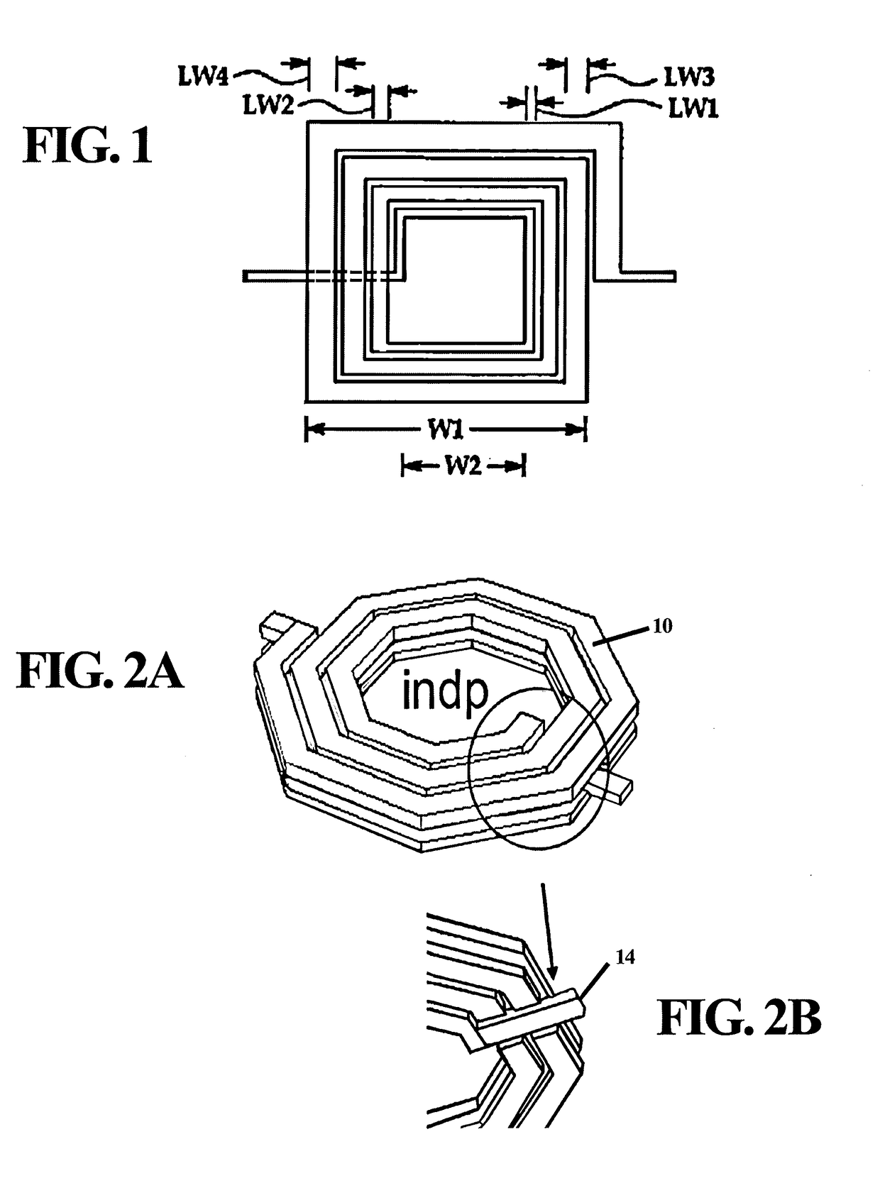
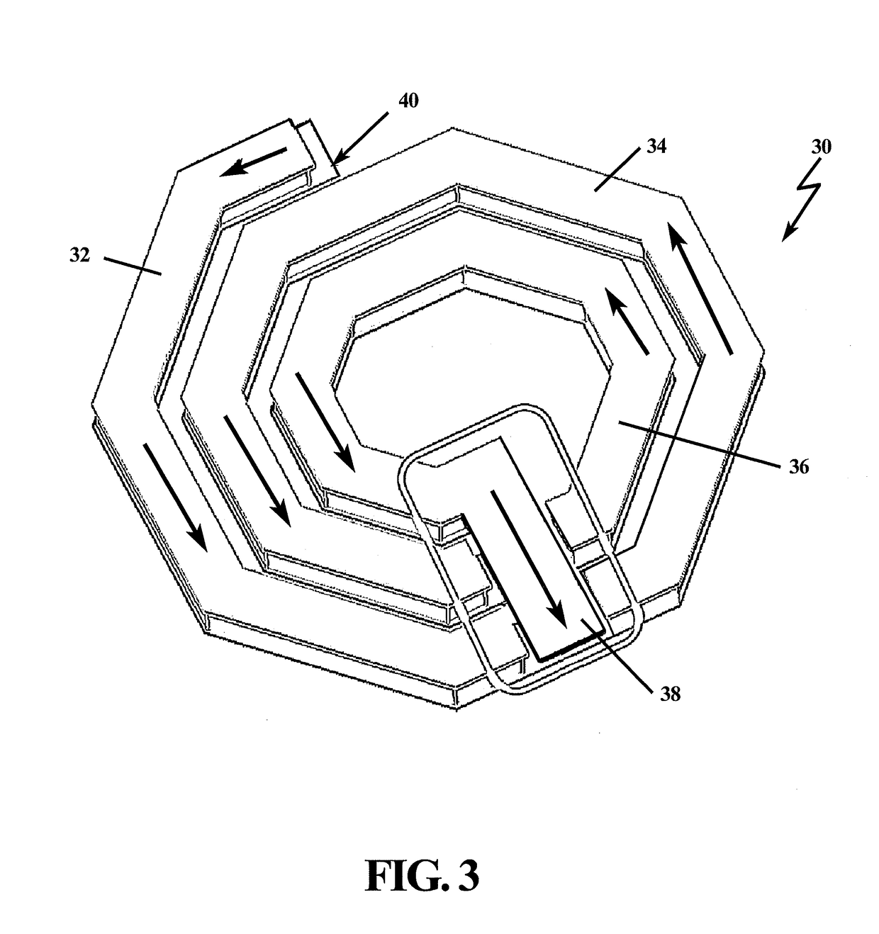
[0010]It is desirable to design and fabricate on-chip inductors with characteristics of small size, high quality factor (Q factor), large inductance, and high self-resonating frequency that are improved from known devices in the art. It is important to make on-chip inductors consume as little real estate as possible to mitigate large parasitic capacitance between the on-chip inductor and the substrate in order to reduce unwanted noise. It is also desirable to introduce an on-chip inductor that achieves a higher Q value for the inductance density and current handling of present RF on-chip inductors.
[0011]Bearing in mind the problems and deficiencies of the prior art, it is therefore an object of the present invention to provide a high efficiency inductor for integrated circuit applications that minimizes the footprint associated with the inductor layout on the substrate.
[0012]It is another object of the present invention to provide a parallel stacked inductor structure which achieves...
PUM
| Property | Measurement | Unit |
|---|---|---|
| width | aaaaa | aaaaa |
| thickness | aaaaa | aaaaa |
| conductive | aaaaa | aaaaa |
Abstract
Description
Claims
Application Information
 - R&D
- Intellectual Property
- Life Sciences
- Materials
- Tech Scout
- Unparalleled Data Quality
- Higher Quality Content
- 60% Fewer Hallucinations
Browse by: Latest US Patents, China's latest patents, Technical Efficacy Thesaurus, Application Domain, Technology Topic, Popular Technical Reports.
© 2025 PatSnap. All rights reserved.Legal|Privacy policy|Modern Slavery Act Transparency Statement|Sitemap|About US| Contact US: help@patsnap.com