

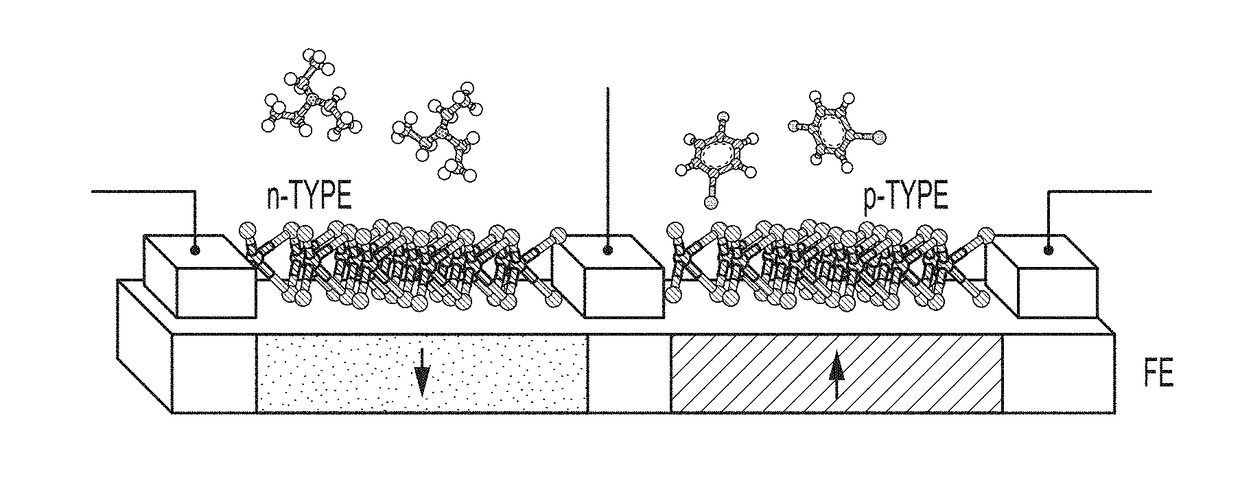
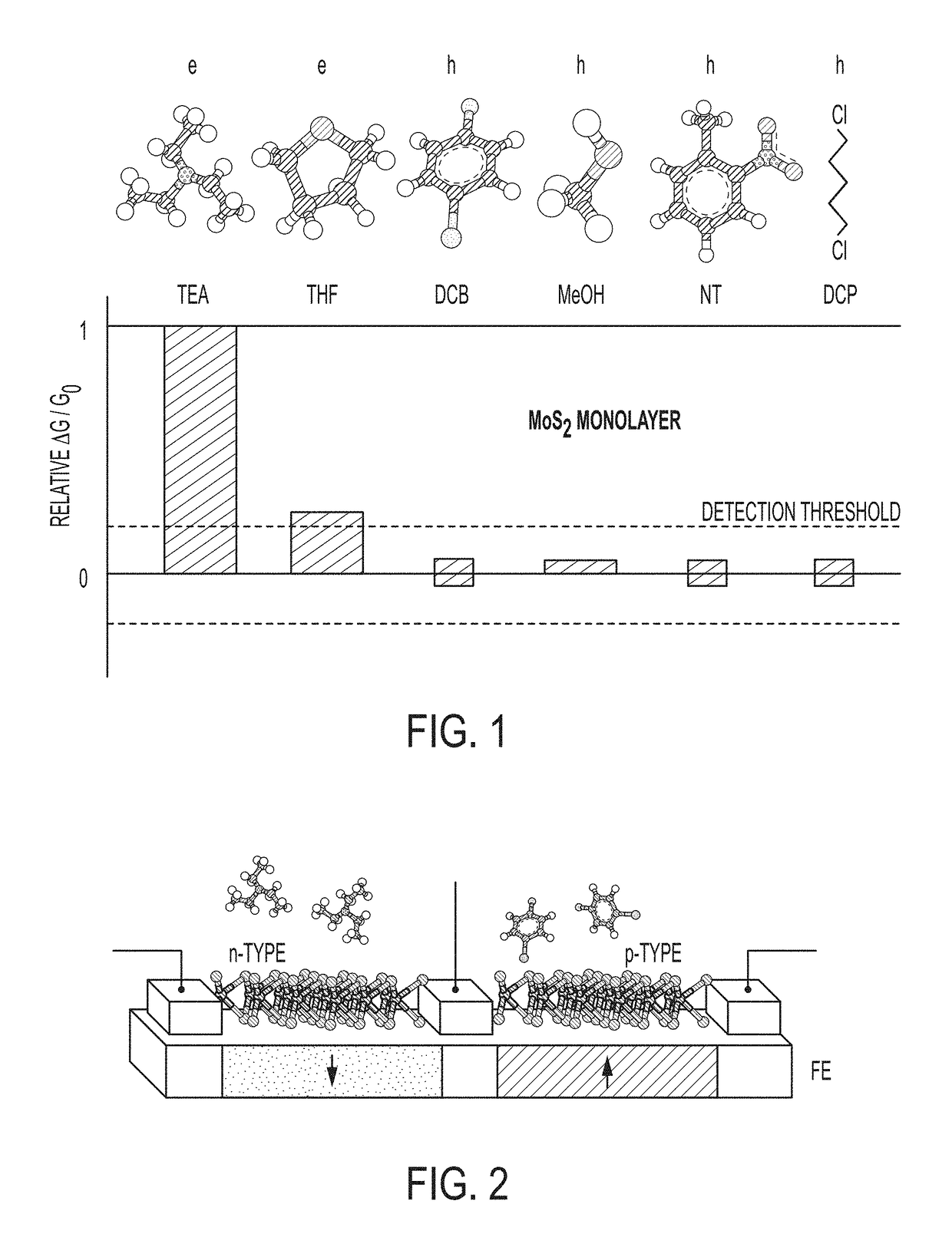
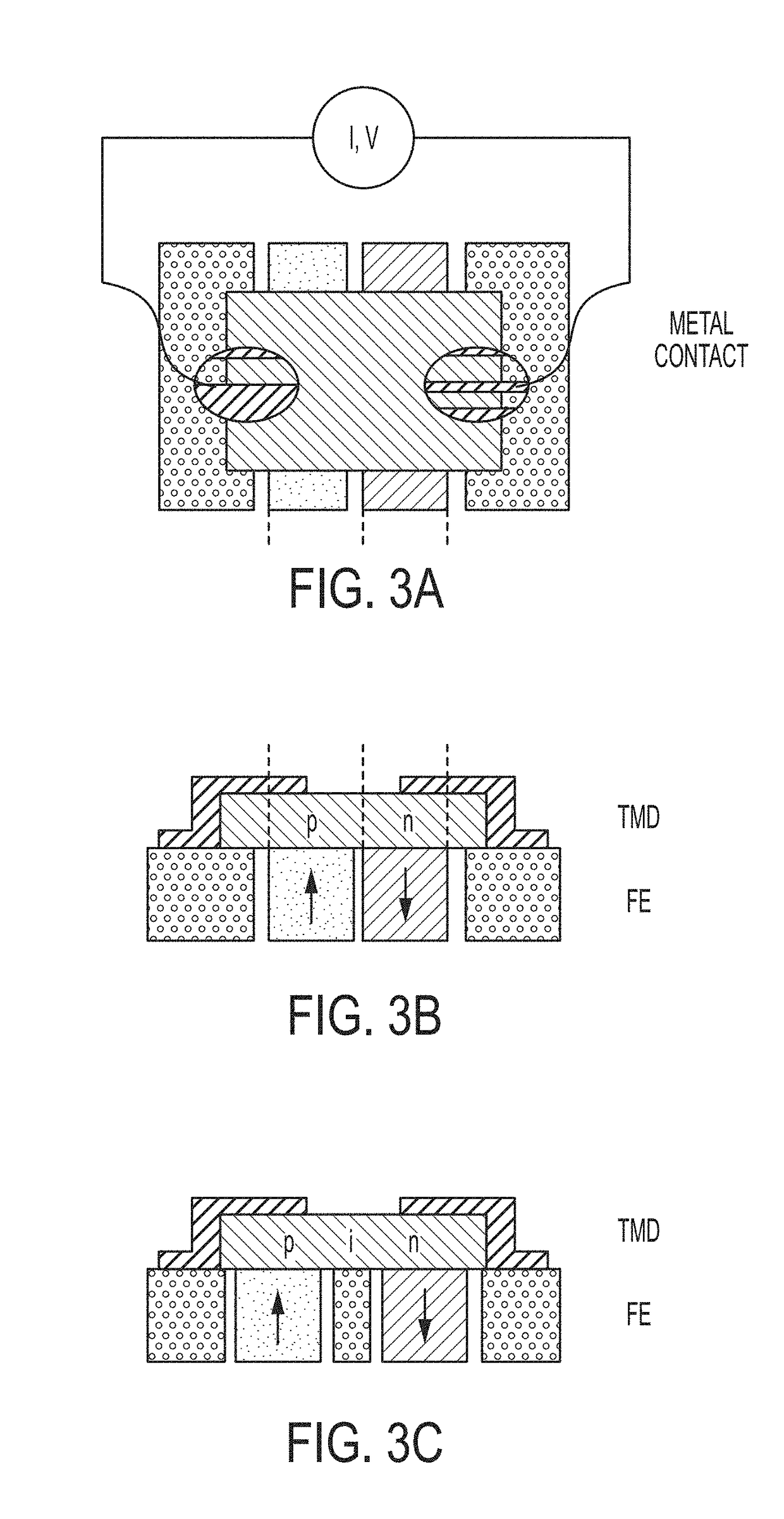
Lateral heterojunctions in two-dimensional materials integrated with multiferroic layers
a two-dimensional material and multi-ferroic layer technology, applied in the field of heterojunctions, can solve the problems of irreversible doping with impurity atoms, inability to change, and inability to change conventional methods,
- Summary
- Abstract
- Description
- Claims
- Application Information
AI Technical Summary
Benefits of technology
Problems solved by technology
Method used
Image

Examples
example 1
[0057]One method for mechanically transferring a TMD monolayer, such as WS2, onto a substrate, such as a ferroelectric film, includes the use of a PMMA film, as illustrated in FIG. 6B. A sample including a layer of WS2 on an SiO2 substrate is coated with a thin layer of PMMA (polymethyl methacrylate) resist and cured on a hot plate at 100° C. for 10 minutes, then submerged in buffered hydrofluoric acid to etch the SiO2, freeing the WS2 from the growth substrate. Once fully etched, the film was rinsed in deionized H2O, where it floated on the surface, and was then lifted from the water using the desired substrate. Optionally, adhesion of the WS2 layer may be improved by spinning at 2000 rpm and baking at 100° C. An acetone and isopropanol soak removes the PMMA. An optical image of PMMA transferred WS2 exhibits a uniform, clean, triangular shape, and is also shown in FIG. 6B.
example 2
[0058]Another method for mechanically transferring a TMD monolayer, such as WS2, onto a substrate, such as a ferroelectric film, includes the use of a PDMS / PC film, as illustrated in FIG. 6C. A sample including a layer of WS2 on an SiO2 substrate is brought into contact a PDMS / PC film, then retracted. This moves the WS2 from Si / SiO2 onto the PDMS / PC film. The PDMS / PC / WS2 stack is then placed onto clean Si / SiO2. The PDMS stamp is retracted, leaving the PC film on the top surface of WS2, which is then dissolved in chloroform. An optical image following PDMS transfer is also shown in FIG. 6C.
example 3
[0059]The carrier type and density in a single monolayer films MoSe2 was controlled by a voltage applied to the electrostatic gate.
[0060]A cross section of a monolayer MoSe2 was grown directly on an SiO2 / Si(001) substrate. A cross-section of the structure is shown in FIG. 7A. The current between the source and drain contacts is determined by the external voltage applied to the gate, where the highly doped Si substrate serves as a gate contact, and the SiO2 serves as the gate dielectric. As shown in FIG. 7B, when the gate voltage is negative, the MoSe2 becomes p-type and the current is dominated by hole motion. When the gate voltage is positive, the MoSe2 becomes n-type and the current is dominated by electron flow. This characteristic is known as “ambipolar.”
[0061]For intermediate voltages, the MoSe2 is depleted of carriers and becomes nearly insulating, with very little current flow. The ratio between the current in the “on” state for electron flow, and the “off” state where curren...
PUM
| Property | Measurement | Unit |
|---|---|---|
| thickness | aaaaa | aaaaa |
| bias voltage | aaaaa | aaaaa |
| bias voltage | aaaaa | aaaaa |
Abstract
Description
Claims
Application Information