Photoelectric conversion element, solid-state imaging device, and electronic apparatus

a technology of photoelectric conversion element and solid-state imaging device, which is applied in the direction of solid-state devices, semiconductor devices, radiation controlled devices, etc., can solve problems such as lowering color reproducibility, and achieve the effects of reducing interaction, and improving the spectroscopic shape of the photoelectric conversion elemen

Active Publication Date: 2018-06-07
SONY SEMICON SOLUTIONS CORP
View PDF4 Cites 7 Cited by
  • Summary
  • Abstract
  • Description
  • Claims
  • Application Information

AI Technical Summary

Benefits of technology

[0013]According to the photoelectric conversion element, the solid-state imaging device, and the electronic apparatus of the respective embodiments of the disclosure, the fullerene derivative modified by a substituent having an absorbance smaller than that of a fullerene in a visible range is used as the semiconductor layer provided between the first electrode and the second electrode that are disposed to face each other. Subjecting a fullerene to polysubstituted modification causes an absorption wavelength peak to be shifted toward shorter wavelength side, and reduces an interaction between fullerenes. This improves the spectroscopic shape of the photoelectric conversion element using the fullerene.
[0014]According to the photoelectric conversion element, the solid-state imaging device, and the electronic apparatus of the respective embodiments of the disclosure, the semiconductor layer provided between the first electrode and the second electrode contains the fullerene derivative modified by a substituent having an absorbance smaller than that of a fullerene in a visible range. Accordingly, the absorption wavelength peak of the fullerene is shifted toward shorter wavelength side, and an interaction between fullerenes are reduced, thus improving the spectroscopic shape of the photoelectric conversion element using the fullerene. In other words, it becomes possible to enhance the photoelectric conversion efficiency of the predetermined wavelength region. It is to be noted that the effects described here are not necessarily limitative, and may be any of effects described in the disclosure.

Problems solved by technology

However, as in the above-described PTLs 2 and 3, in a case where the photoelectric conversion layer itself has a spectroscopic function, when simply using the fullerene or the fullerene derivative as the photoelectric conversion layer, there is an issue of a deteriorated spectroscopic shape of the photoelectric conversion element due to a broad absorption spectrum of the fullerene, which leads to lowered color reproducibility.

Method used


Image

  • Photoelectric conversion element, solid-state imaging device, and electronic apparatus
  • Photoelectric conversion element, solid-state imaging device, and electronic apparatus
  • Photoelectric conversion element, solid-state imaging device, and electronic apparatus

Examples


embodiment

1. Embodiment

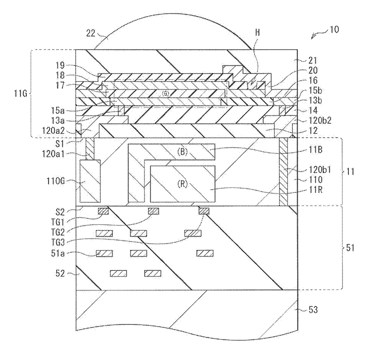
[0041]FIG. 1 illustrates a cross-sectional configuration of a photoelectric conversion element (photoelectric conversion element 10) according to an embodiment of the disclosure. The photoelectric conversion element 10 constitute a single pixel in, for example, a solid-state imaging device (described later) such as a CCD image sensor and a CMOS image sensor. The photoelectric conversion element 10 includes, on side of a front surface (surface S2 opposite to light-receiving surface) of a semiconductor substrate 11, pixel transistors (including transfer transistors Tr1 to Tr3 described later) formed as well as a multi-layer wiring layer (multi-layer wiring layer 51).

[0042]The photoelectric conversion element 10 of the present embodiment has a structure in which one organic photoelectric conversion section 11G and two inorganic photoelectric conversion sections 11B and 11R are stacked in a vertical direction. The organic photoelectric conversion section 11G selectively det...

application examples

2. APPLICATION EXAMPLES

Application Example 1

[0104]FIG. 14 illustrates an overall configuration of the solid-state imaging device (solid-state imaging device 1) that uses, as each pixel, the photoelectric conversion element 10 described in the foregoing embodiment. The solid-state imaging device 1 is a CMOS imaging sensor. The solid-state imaging device 1 has a pixel section la as an imaging region on the semiconductor substrate 11. Further, the solid-state imaging device 1 includes, for example, a peripheral circuit section 130 configured by a row scanning section 131, a horizontal selection section 133, a column scanning section 134, and a system controller 132 in a peripheral region of the pixel section 1a.

[0105]The pixel section la includes, for example, a plurality of unit pixels P (corresponding to photoelectric conversion elements 10) that are arranged two-dimensionally in matrix. To the unit pixels P, for example, pixel drive lines Lread (specifically, row selection lines an...

application example 2

[0110]The above-described solid-state imaging device 1 is applicable to any type of electronic apparatus having an imaging function, for example, a camera system such as a digital still camera and a video camera, and a mobile phone having the imaging function. FIG. 14 illustrates an outline configuration of an electronic apparatus 2 (camera) as an example thereof. This electronic apparatus 2 may be, for example, a video camera that is able to photograph a still image or a moving image. The electronic apparatus 2 includes, for example, the solid-state imaging device 1, an optical system (optical lens) 310, a shutter device 311, a drive section 313 that drives the solid-state imaging device 1 and the shutter device 311, and a signal processing section 312.

[0111]The optical system 310 guides image light (incident light) from a subject to the pixel section la in the solid-state imaging device 1. The optical system 310 may be configured by a plurality of optical lenses. The shutter devic...


PUM


Abstract

A photoelectric conversion element according to an embodiment of the disclosure includes a first electrode and a second electrode, and an organic semiconductor layer. The first electrode and the second electrode are disposed to face each other. The organic semiconductor layer is provided between the first electrode and the second electrode, and contains a fullerene derivative modified by a substituent having an absorbance smaller than that of a fullerene.

Description

TECHNICAL FIELD[0001]The disclosure relates to, for example, a photoelectric conversion element using an organic semiconductor, a solid-state imaging device provided with the photoelectric conversion element, and an electronic apparatus.BACKGROUND ART[0002]In recent years, there has been progress in miniaturization of a pixel size in a solid-state imaging device such as a charge coupled device (CCD) image sensor and a complementary metal oxide semiconductor (CMOS) image sensor. This leads to a decrease in the number of photons that enter a unit pixel, thus leading to lowered sensitivity as well as a lowered S / N ratio. Further, in a case of using a color filter in which primary color filters of red, green, and blue are two-dimensionally arrayed for colorization, pieces of light of green and blue are absorbed by the color filter in a red pixel, thus causing the sensitivity to be lowered. Furthermore, an interpolation process is performed between pixels upon generation of each color si...

Claims


Application Information

Patent Timeline
Patent Type & Authority Applications(United States)
IPC IPC(8): H01L51/44H01L31/0224H01L27/146
CPCH01L51/441H01L31/022425H01L27/14609H01L27/14603H01L27/1464H01L27/14645H01L27/14667Y02E10/549H04N25/70H04N23/10H10K39/32H10K85/215H10K85/311H10K30/00H01L31/10H10K30/81
Inventor TAKEMURA, ICHIRONEGISHI, YUKIHASEGAWA, YUTA
Owner SONY SEMICON SOLUTIONS CORP
Why Eureka
Try Eureka