BOOTSTRAP CAPACITOR OVER-VOLTAGE MANAGEMENT CIRCUIT FOR GaN TRANSISTOR BASED POWER CONVERTERS

a technology of gan transistors and power converters, which is applied in the direction of pulse techniques, process and machine control, instruments, etc., can solve the problems of overcharging of bootstrap capacitors, and achieve the effect of low voltage drop path

Active Publication Date: 2018-06-07
EFFICIENT POWER CONVERSION CORP
View PDF9 Cites 30 Cited by
  • Summary
  • Abstract
  • Description
  • Claims
  • Application Information

AI Technical Summary

Benefits of technology

[0020]The present invention provides a modified drive circuit for a half bridge transistor circuit that avoids the gate drive overvoltage condition described above, and overcomes the above-noted deficiencies of the prior art, by providing a shunt diode connected to the bootstrap capacitor at a node VB between the bootstrap capacitor and ground, the shunt diode being decoupled from the midpoint node of the half bridge (VSW) by a shunt resistor. The shunt diode advantageously provides a low voltage drop path to charge the bootstrap capacitor during the dead-time charging period when both the high side and low side transistors of the half bridge are off. The shunt resistor controls and limits the current through the shunt diode.

Problems solved by technology

The large reverse conduction voltage drop of the GaN transistor will result in overcharging of the bootstrap capacitor.

Method used


Image

  • BOOTSTRAP CAPACITOR OVER-VOLTAGE MANAGEMENT CIRCUIT FOR GaN TRANSISTOR BASED POWER CONVERTERS
  • BOOTSTRAP CAPACITOR OVER-VOLTAGE MANAGEMENT CIRCUIT FOR GaN TRANSISTOR BASED POWER CONVERTERS
  • BOOTSTRAP CAPACITOR OVER-VOLTAGE MANAGEMENT CIRCUIT FOR GaN TRANSISTOR BASED POWER CONVERTERS

Examples


third embodiment

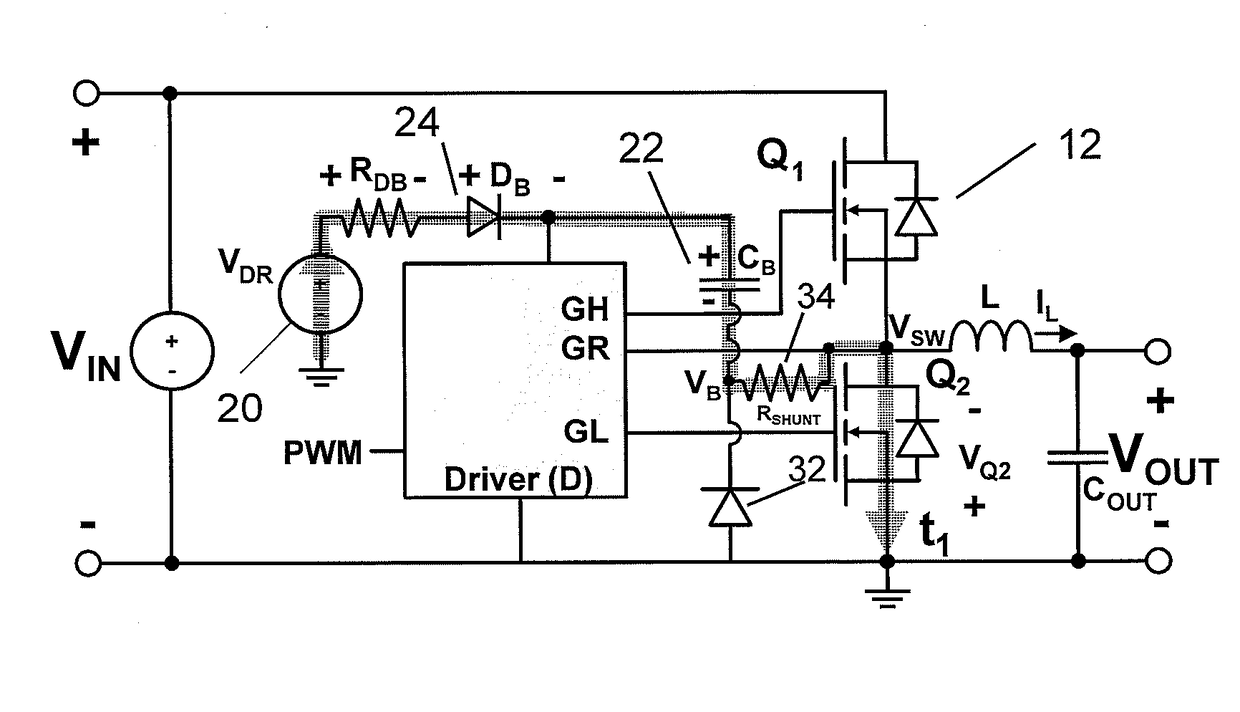
[0039]In the invention, shown in FIG. 5, a second shunt diode 52 (DSHUNT2) is inserted in series with shunt resistor (RSHUNT) to provide additional control over the effective impedance and voltage drop.

[0040]As shown in FIG. 6, in a fourth embodiment, the present invention is extended to converters with a higher number of levels. The implementation of the first embodiment of the present invention is shown in FIG. 6, but the other embodiments of the invention described herein can also be extended to converters with a higher number of levels in a similar fashion.

fifth embodiment

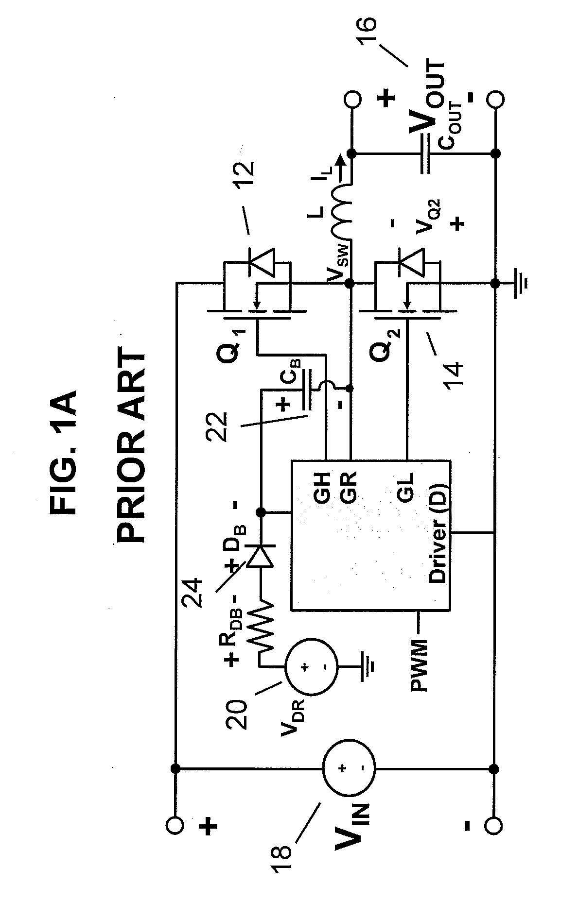
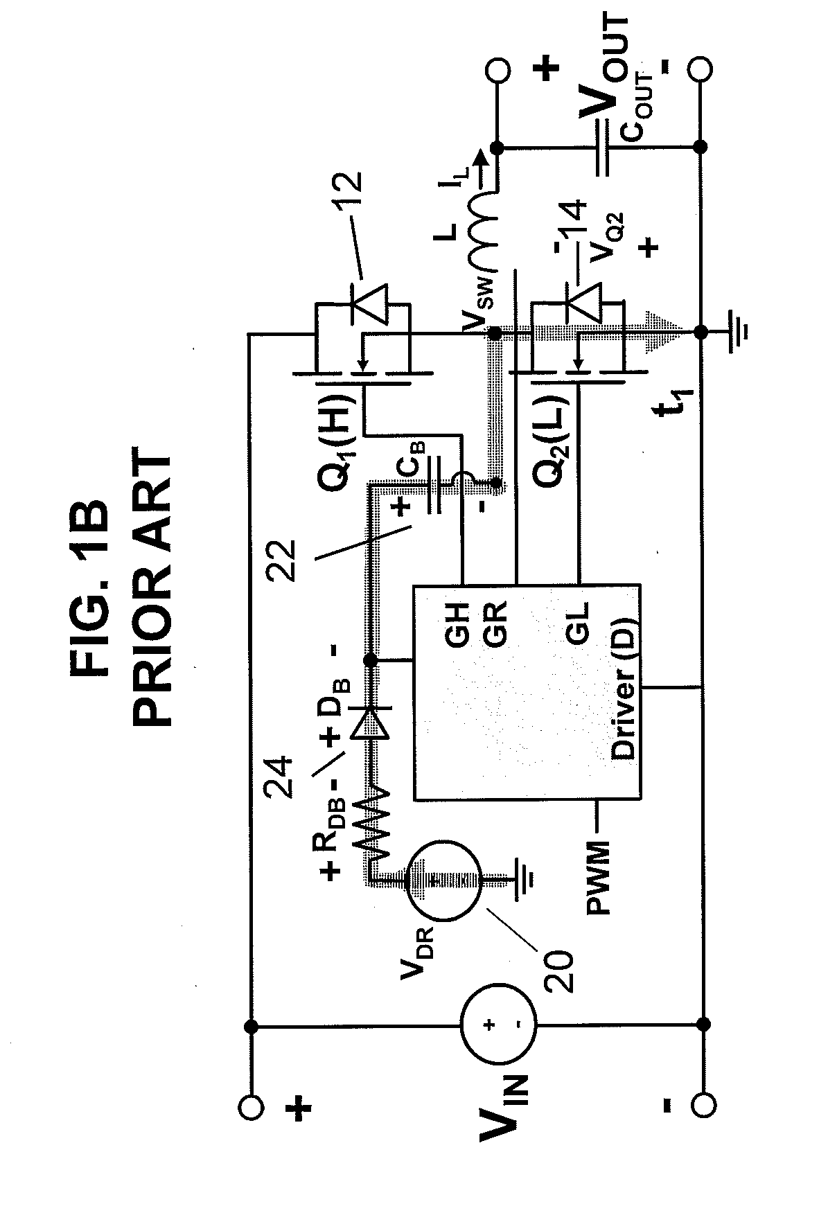
[0041]In the present invention, shown in FIGS. 7A and 7B, shunt diode 32 (DSHUNT) can be replaced with an active semiconductor, i.e., transistor 70 (QSHUNT), which is driven with the complementary gate drive signal of transistor 12 (Q1). U.S. Pat. No. 8,536,847, incorporated by reference herein, discloses a circuit in which a transistor Q3 is employed in a similar fashion in a bootstrap drive circuit, but the circuit of this patent requires a complicated reference voltage circuit because the power pin and the gate drive pin are referenced to different potentials. If referenced at same potential, there would be no balancing method to limit power current from conducting in the smaller Q3. In contrast, in the present invention, the shunt resistor 34 (RSHUNT) simply provides impedance to control the charging ratio between transistor 70 (QSHUNT) and low side transistor 14 (Q2), which are both referenced to GND, while allowing a direct connection of the power and gate drive pins, without ...


PUM


Abstract

A drive circuit for a half bridge transistor circuit formed of enhancement mode GaN transistors. A shunt diode is connected to the bootstrap capacitor at a node between the bootstrap capacitor and ground, the shunt diode being decoupled from the midpoint node of the half bridge by a shunt resistor. The shunt diode advantageously provides a low voltage drop path to charge the bootstrap capacitor during the dead-time charging period when both the high side and low side transistors of the half bridge are off.

Description

[0001]This application claims the benefit of U.S. Provisional Application No. 62 / 428,854, filed Dec. 1, 2016, the entire disclosure of which is hereby incorporated by reference in its entirety.BACKGROUND OF THE INVENTION[0002]Since their inception, normally off enhancement mode (e-mode) gallium nitride (GaN) transistors have demonstrated superior in-circuit performance compared to conventional silicon technologies. E-mode GaN transistors, and wide bandgap power devices in general, are capable of higher performance than silicon MOSFET technology and have led to the development of improved applications fundamentals to fully utilize the capability of the superior power devices and better optimize designs around the unique device properties.[0003]For e-mode GaN transistors, one distinct device property is a lower maximum gate voltage capability when compared to standard silicon MOSFETs. Specifically, the gate overhead margin, which is defined as the difference between the manufacturers ...

Claims


Application Information

Patent Timeline
Patent Type & Authority Applications(United States)
IPC IPC(8): H03K17/687G05F1/571H03K17/567H03K17/06H03K17/0812H02M1/32H01L29/20H02M3/158H03K17/042
CPCH03K17/6871G05F1/571H03K17/567H03K17/063H03K17/08122H02M1/32H01L29/2003H02M3/158H03K17/04206H03K2217/0072H02M2001/0003H03K2217/0063H03K2217/0081H01L29/7801H02M1/0006Y02B70/10H02M1/0003
Inventor REUSCH, DAVID C.GLASER, JOHNDE ROOIJ, MICHAEL A.
Owner EFFICIENT POWER CONVERSION CORP
Why Eureka
Try Eureka