

Quartz crystal microbalance utilization for foreline solids formation quantification
a quartz crystal microbalance and foreline solids technology, applied in the direction of perfluorocarbon/hydrofluorocarbon capture, sustainable manufacturing/processing, final product manufacturing, etc., can solve the problems of inability to remove pfcs from effluent, unfavorable environmental release, pump failure and foreline clogging
- Summary
- Abstract
- Description
- Claims
- Application Information
AI Technical Summary
Benefits of technology
Problems solved by technology
Method used
Image

Examples
Embodiment Construction
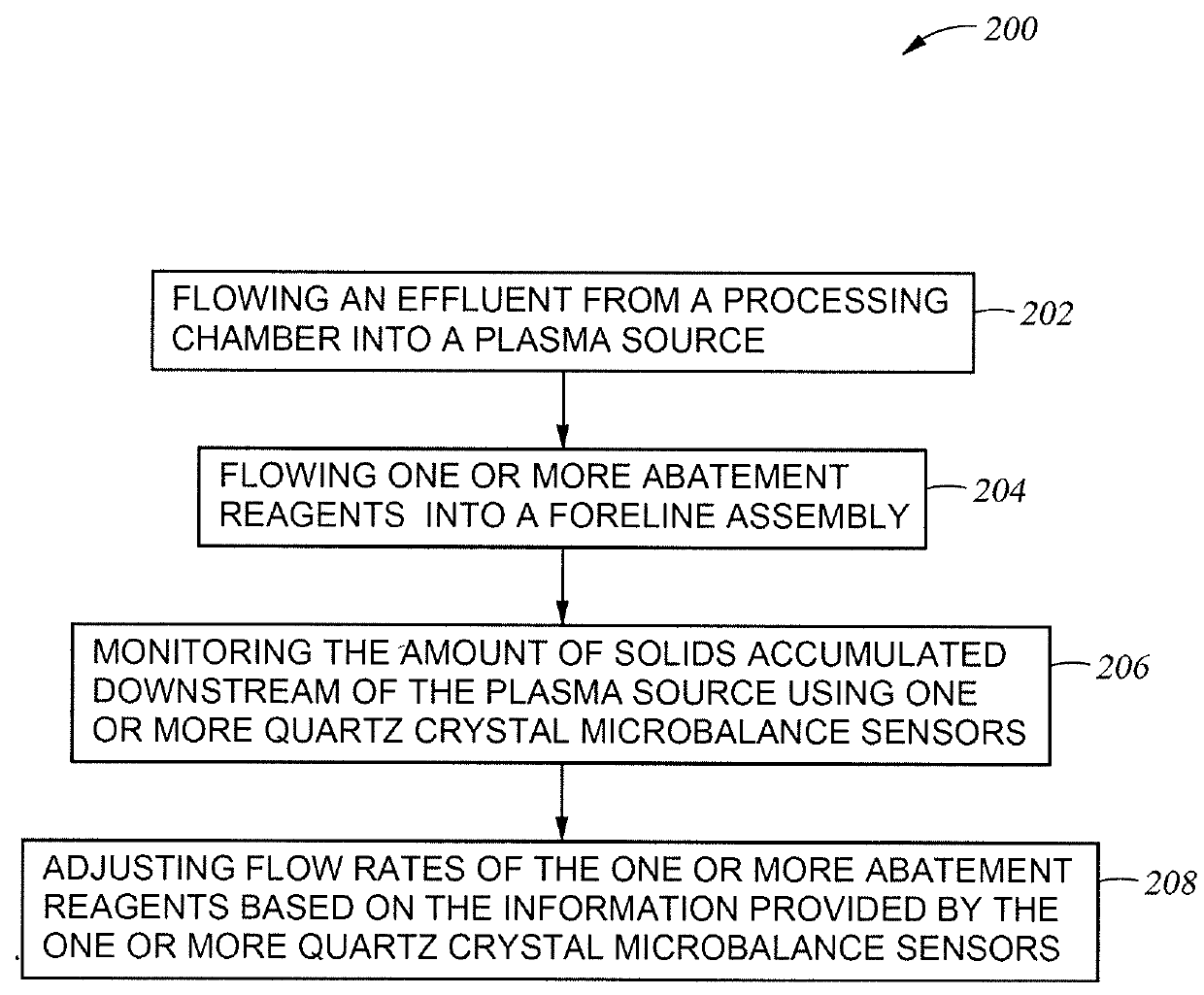
[0015]Embodiments of the present disclosure generally relate to abatement for semiconductor processing equipment. More particularly, embodiments of the present disclosure relate to techniques for foreline solids formation quantification. In one embodiment, a system includes one or more quartz crystal microbalance (QCM) sensors located between a processing chamber and a facility exhaust. The one or more QCM sensors provide real-time measurement of the amount of solids generated in the system without having to shut down a pump located between the processing chamber and the facility exhaust. In addition, information provided by the QCM sensors can be used to control the flow of reagents used to abate compounds in the effluent exiting the processing chamber in order to reduce solid formation.
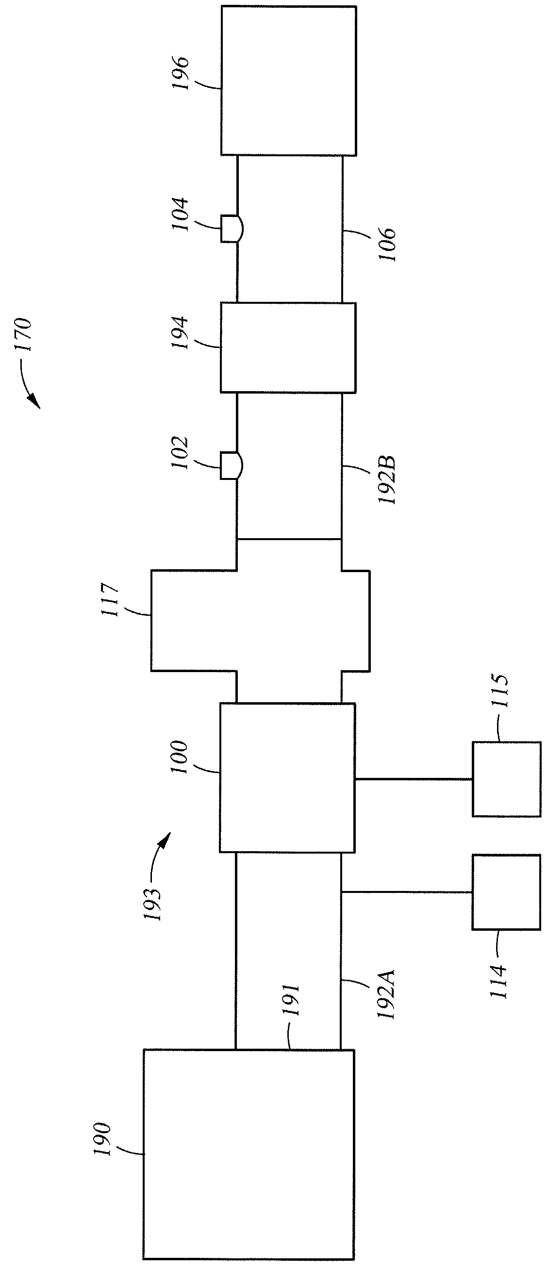
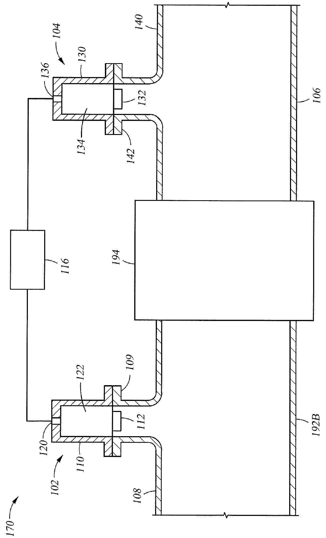
[0016]FIG. 1A is a schematic side view of a vacuum processing system 170. The vacuum processing system 170 includes at least a vacuum processing chamber 190, a vacuum pump 194, and a foreline assemb...
PUM
| Property | Measurement | Unit |
|---|---|---|
| plasma | aaaaa | aaaaa |
| flow rates | aaaaa | aaaaa |
| flow rate | aaaaa | aaaaa |
Abstract
Description
Claims
Application Information