Methods and devices for monitoring and controlling thin film processing

a technology of thin film and monitoring device, applied in the direction of vacuum evaporation coating, chemical vapor deposition coating, coating, etc., can solve the problem that the optical monitoring of the deposited layer cannot provide any useful information, the composition or optical properties of the deposited layer cannot be directly measured, and the performance of the device manufactured using thin film deposition methods is impeded. problem, to achieve the effect of reducing process errors, eliminating or reducing process errors

Active Publication Date: 2010-11-09
EXCELITAS TECH
View PDF31 Cites 18 Cited by
  • Summary
  • Abstract
  • Description
  • Claims
  • Application Information

AI Technical Summary

Benefits of technology

[0013]The present invention provides thin film processing systems for fabricating thin films and devices comprising thin films having accurate thin film layer control with respect to the physical thickness, thickness profile, chemical composition and physical characteristics of deposited thin film layers. The present invention comprises thin film processing methods and devices for depositing precursors onto a substrate that are capable of generating thin film layers and multilayer structures comprising thin film layers having accurately selected physical thicknesses, thickness profiles, chemical compositions and physical properties. Thin film processing monitoring systems and methods are provided that provide real time, in situ measurements of the mass, physical thickness, refractive index, optical thickness, surface morphology and / or electrical charge characteristics of a thin film layer deposited onto a sensor undergoing translation and / or rotation that is substantially coincident with the translation and / or rotation of a substrate in a flux region of a thin film processing system. The present invention also provides thin film layer monitoring and control methods for making single layer and multilayer structures comprising thin film layers having spatially uniform physical thicknesses or thin film layers having selected non-uniform thickness profiles with improved accuracy and precision relative to conventional thin film processing systems. Further, methods and systems of the present invention eliminate reliance on characterization of a parts-to-monitor ratio. Methods and systems of the present invention employing an onboard sensor with supporting electrical circuitry and having a wireless transmitter are capable of providing measurements of processing characteristics representative of thin film processing on a substrate surface while moving in a flux region of a thin film processing system along virtually any trajectory including complex trajectories substantially coincident with the trajectories of one or more substrates in a planetary system, such as a dual rotation planetary system.

Problems solved by technology

Such variability in the thickness of deposited thin film layers can impede the performance of devices fabricated using thin film deposition methods.
In contrast to crystal monitoring, optical techniques do not provide a direct measurement of physical properties (e.g. mass or physical thickness) of the deposited layers.
For example, in situations where a thin film layer is deposited on top of a pre-existing structure of uncertain physical dimensions, composition or optical properties optical monitoring does not provide useful information in all cases.
Even in the case of deposition of a thin film layer on an uncoated, well defined substrate surface, layer thickness errors from optical monitoring can oscillate out of control, and optically insensitive layers can lead to layer thickness errors that become important when an entire structure is complete.
Finally, optical monitoring is often susceptible to problems associated with substrate heating and etalon effects in a given optical system.
Optical monitoring also fails when appropriate light sources and detection systems are not available.
Quartz crystal monitoring as currently practiced, however, does not provide a direct measurement of the mass of materials actually deposited on a substrate.
As a result of this experimental limitation, conventional crystal monitoring techniques typically employ a fixed position crystal monitor at a location proximate to the substrate surface undergoing deposition.
This drift results in layer thickness errors which can significantly degrade the quality and / or performance of thin film devices and device components fabricated via thin film deposition methods.
In addition, these methods require derivation of complex mathematical relationships relating a measured source distribution profile of precursors to motion scenarios of substrates required to achieve good uniformity.
Mobile source processing monitor configurations described in U.S. Pat. No. 4,858,556 are limited to embodiments using “a sliding contact electrical interface 152 (FIG. 7)” which makes complex monitor trajectories, such as dual rotation trajectories, impractical and / or unfeasible.
It is very difficult to control the stability of the electrical sensing circuitry in this arrangement due to anticipated changes in conductivity, capacitance, resistance and impedance upon rotation or sliding motion of the electrical contacts.
Therefore, this arrangement is expected to be susceptible to substantial errors in the measured layer thicknesses arising from the sliding or rotating electrical contacts.
Moreover, the configurations disclosed in this reference are not amenable to high-throughput fabrication applications.

Method used


Image

  • Methods and devices for monitoring and controlling thin film processing
  • Methods and devices for monitoring and controlling thin film processing
  • Methods and devices for monitoring and controlling thin film processing

Examples


example 1

Film Thickness Monitoring and Control Methods Using an Optical Sensor

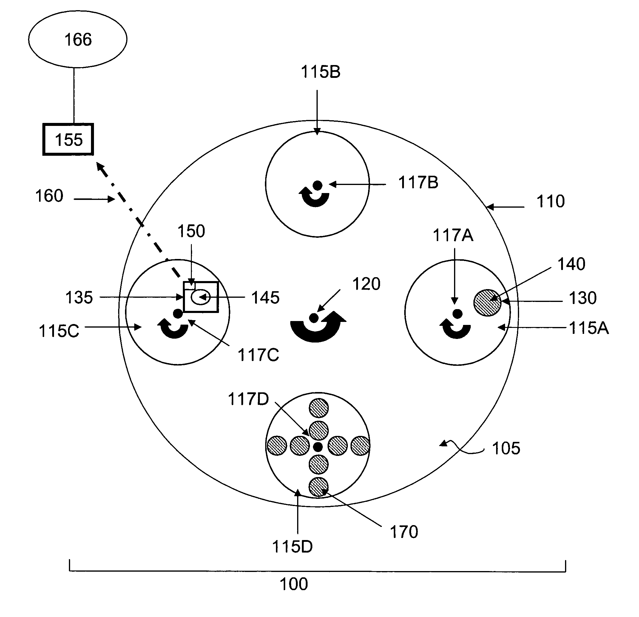
[0116]The present invention includes methods and devices having a moving optical sensor that is capable of movement along a trajectory in a flux region of a thin film processing system that is substantially coincident with the trajectories of one or more substrates undergoing translation and / or rotating during thin film processing. FIG. 9A shows a schematic diagram illustrating a moveable optical sensor of the present invention for positioning on a means for translating the sensor in the flux region of a thin film processing system. Moveable optical sensor 700 comprises optical source 705, sensor substrate 710, detector 715, and wireless transmitter 716. Each of these elements are provided in housing element 717, which is capable of integration with a means of translation, such as integration with a sub-planet of a dual rotation planetary system.

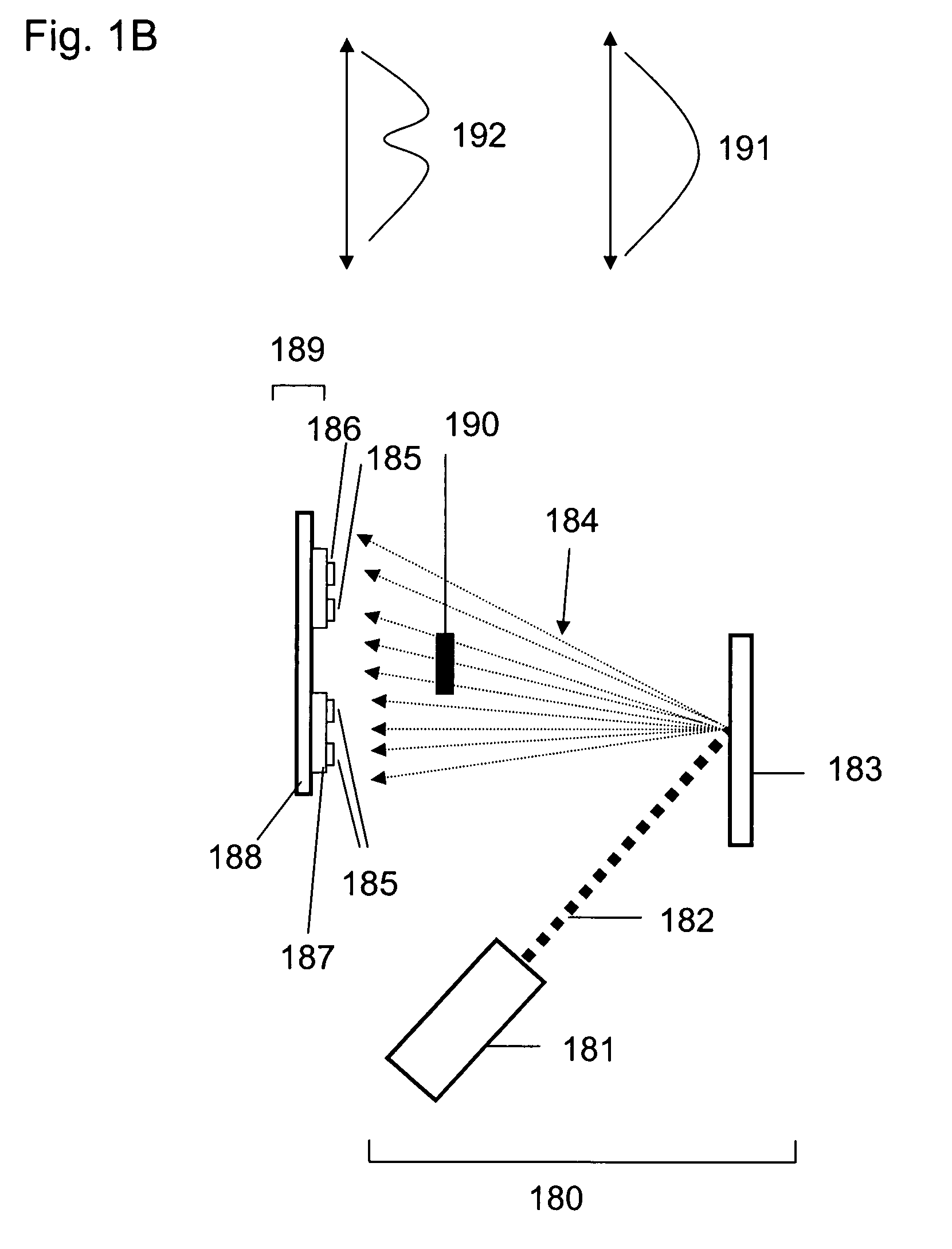
[0117]Optical source 705 generates optical beam 706 that is directed o...

example 2

Film Thickness Monitoring and Control Methods Incorporating an SC Cut Quartz Crystal Monitor

[0122]Thin film processing systems and related methods of the present invention having a deposition sensor that moves along a trajectory that is substantially coincident with the trajectories of substrates undergoing processing enables realization of significant further improvements in film thickness control. In one embodiment, thin film processing systems of the present invention further comprise a moveable quartz crystal microbalance deposition sensor having a doubly rotated cut, such as an SC-cut, capable of operation in a manner that is significantly less susceptible to film thickness errors arising from changes in the temperature of the sensor and stress exerted on the sensor by deposited films than conventional AT cut quartz crystal deposition sensors. Use of a moveable SC-cut quartz crystal microbalance deposition sensor capable of movement along a trajectory substantially coincident w...


PUM

PropertyMeasurementUnit
diameteraaaaaaaaaa
thicknessaaaaaaaaaa
distanceaaaaaaaaaa

Abstract

Thin film processing systems and methods are provided having a moving deposition sensor capable of translation and / or rotation in a manner that exposes the sensor to thin film deposition environments in a flux region substantially the same as the deposition environments experienced by one or more moveable substrates during a selected deposition period. In one embodiment, a thin film monitoring and control system is provided wherein one or more moveable substrates and a moveable deposition sensor are moved along substantially coincident trajectories in a flux region of a thin film deposition system for a selected deposition period. Systems and methods of the present invention may include SC-cut quartz crystal microbalance sensors capable of excitation of at least two different resonant modes.

Description

CROSS-REFERENCE TO RELATED APPLICATIONS[0001]This application claims priority under 35 U.S.C. 119(e) to U.S. provisional Patent Application 60 / 640,539 filed Dec. 30, 2004, which is hereby incorporated by reference in its entirety to the extent not inconsistent with the disclosure herein.BACKGROUND OF THE INVENTION[0002]Thin film deposition methods enable the fabrication of a wide range of useful devices and device components. Chemical and physical thin film deposition techniques, such as ion beam sputtering, plasma enhanced chemical thin film deposition, electron beam evaporation and thermal evaporation, for example, are particularly useful methods for fabricating complex structures comprising thin films of a variety of materials, including dielectric materials, semiconductors, and conducting materials. Structures have been fabricated using thin film deposition methods having selected thicknesses ranging from 10 s of nanometers to 10 s of centimeters. The applicability of thin film ...

Claims


Application Information

Patent Timeline
Patent Type & Authority Patents(United States)
IPC IPC(8): C23F1/00H01L21/306
CPCC23C14/505C23C14/546C23C14/547C23C16/4584C23C16/52C23C14/54C23C16/458
Inventor LEE, WILLIAM DAVIDNESS, DALE C.STREATER, ALAN D.
Owner EXCELITAS TECH
Why Eureka
Try Eureka