Semiconductor device and electronic device including the semiconductor device

a semiconductor and electronic technology, applied in static indicating devices, instruments, biological models, etc., can solve the problems of increasing the cost of components such as wirings and power required for transmitting image data, and achieve the effect of small circuit area and low power consumption

Active Publication Date: 2018-07-26
SEMICON ENERGY LAB CO LTD
View PDF9 Cites 42 Cited by
  • Summary
  • Abstract
  • Description
  • Claims
  • Application Information

AI Technical Summary

Benefits of technology

[0010]In a television that has received a signal for 8K broadcasting, for example, the received broadcast signal is decompressed (decoded) to obtain an enormous amount of data corresponding to an 8K image. In the case of transmitting such an enormous amount of image data to a display device, the number of wirings used for transmitting the image data is increased as the resolution of the display device becomes higher. Thus, the cost for components such as the wirings and power required for transmitting image data are increased.
[0012]Another object of one embodiment of the present invention is to provide a semiconductor device with a small circuit area. Another object of one embodiment of the present invention is to provide a semiconductor device with low power consumption. Another object of one embodiment of the present invention is to provide a semiconductor device capable of performing high-speed arithmetic processing.
[0026]Another embodiment of the present invention can provide a semiconductor device with a small circuit area. Another embodiment of the present invention can provide a semiconductor device with low power consumption. Another embodiment of the present invention can provide a semiconductor device capable of performing high-speed arithmetic processing.

Problems solved by technology

Thus, the cost for components such as the wirings and power required for transmitting image data are increased.

Method used


Image

  • Semiconductor device and electronic device including the semiconductor device
  • Semiconductor device and electronic device including the semiconductor device
  • Semiconductor device and electronic device including the semiconductor device

Examples


embodiment 1

[0087]In this embodiment, the configuration of a source driver circuit that is a semiconductor device of one embodiment of the present invention will be described.

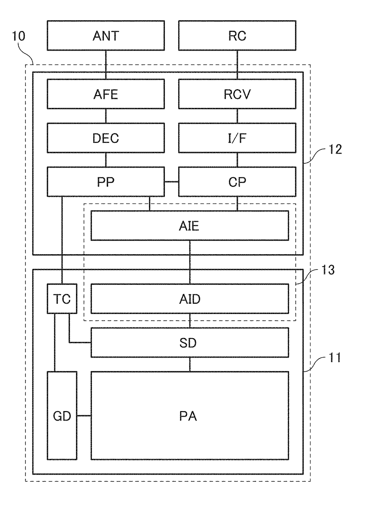
[0088]FIG. 1 is a block diagram of an electronic device including a display device, a receiver, and the like. An electronic device 10 includes a display device 11 and a receiver 12. FIG. 1 also illustrates an antenna ANT that receives a broadcast signal and a remote controller RC that is used for the control of the electronic device 10.

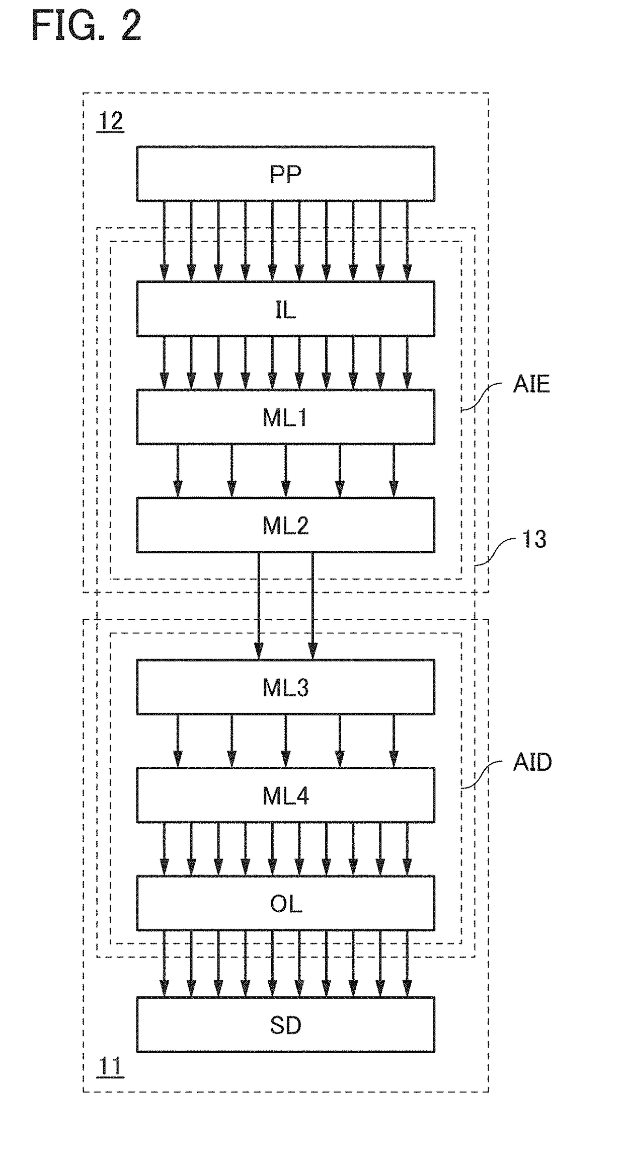
[0089]The display device 11 includes a display portion PA, a gate driver circuit GD, a source driver circuit SD, a timing controller TC, and an artificial intelligence (AI) decoder AID.

[0090]The receiver 12 includes a receive portion RCV, an interface I / F, a control portion CP, an analog front end AFE, a decoder DEC, an image processing portion PP, and an AI encoder AIE.

[0091]Note that in the electronic device 10, the AI decoder AID included in the display device 11 and the AI encoder AIE in...

embodiment 2

[0205]In this embodiment, a configuration example of the autoencoder described in the above embodiment will be described. Specifically, a configuration example in which a convolutional neural network (CNN) is used for the feature extraction in the AI encoder will be described.

[0206]FIG. 8 illustrates a configuration example of the CNN. The CNN includes a convolution layer CL, a pooling layer PL, and a fully connected layer FCL. In the case of using the CNN in the AI encoder AIE, image data IPD output from the image processing portion PP is input to the CNN and then the feature extraction is performed.

[0207]The convolution layer CL has a function of performing convolution on the image data. In the convolution, the product-sum operation using part of the image data and the filter value of a weight filter is repeatedly performed. As a result of the convolution by the convolution layer CL, a feature of an image is extracted.

[0208]For the convolution, one weight filter or a plurality of ...

embodiment 3

[0257]In this embodiment, a configuration example of a display panel including the semiconductor device described in Embodiment 1 will be described.

[0258]FIG. 17 illustrates a configuration example of a display panel including the source driver circuit SD described in Embodiment 1. In a display panel 20, the display portion PA is formed over a substrate 21. The display portion PA includes a plurality of pixels 22 electrically connected to wirings GAL and wirings SOL.

[0259]Note that the pixels 22 correspond to the pixels included in the display portion PA illustrated in FIG. 3, the pixels PIX[1] and PIX[2] illustrated in FIG. 4, or the pixels PIX[1] to PIX[x] illustrated in FIG. 7, which are described in Embodiment 1. In the case where one wiring GAL is electrically connected to pixels in a plurality of rows, the wiring GAL corresponds to the wiring GWL, which is illustrated in FIG. 4 and FIG. 7 and described in Embodiment 1.

[0260]The display panel 20 is provided with a plurality of ...


PUM


Abstract

A semiconductor device with a small circuit area that consumes low power is provided. The semiconductor device includes a shift register, a sample-and-hold circuit, a first buffer circuit, and a second buffer circuit. The sample-and-hold circuit includes a first input terminal, a second input terminal, and an output terminal. An output terminal of the first buffer circuit is electrically connected to the first input terminal. The shift register is electrically connected to the second input terminal. An input terminal of the second buffer circuit is electrically connected to the output terminal of the sample-and-hold circuit. In the semiconductor device, the potential of an input analog signal is retained in the sample-and-hold circuit and the analog signal is output from an output terminal of the second buffer circuit.

Description

TECHNICAL FIELD[0001]One embodiment of the present invention relates to a semiconductor device and an electronic device including the semiconductor device.[0002]Note that one embodiment of the present invention is not limited to the above technical field. The technical field of the invention disclosed in this specification and the like relates to an object, a method, or a manufacturing method. One embodiment of the present invention relates to a process, a machine, manufacture, or a composition of matter. Specifically, examples of the technical field of one embodiment of the present invention disclosed in this specification include a semiconductor device, a display device, a liquid crystal display device, a light-emitting device, a power storage device, an imaging device, a memory device, a processor, an electronic device, a system, a method for driving any of them, a method for manufacturing any of them, and a method for inspecting any of them.BACKGROUND ART[0003]A demand for high-...

Claims


Application Information

Patent Timeline
Patent Type & Authority Applications(United States)
IPC IPC(8): G09G3/36H01L29/786H01L27/12G11C27/04G11C27/02
CPCG09G3/3674H01L29/78648H01L27/1251H01L29/7869G11C27/04G11C27/024G06N3/04G06N3/08G09G2310/0286G09G2310/0294G09G2310/0291G09G2310/0297G09G3/3688G11C19/184G09G3/3677H01L27/1225G06N3/063G06N3/084G06N3/048G06N3/045
Inventor KUROKAWA, YOSHIYUKIIKEDA, TAKAYUKIINOUE, TATSUNORI
Owner SEMICON ENERGY LAB CO LTD
Why Eureka
Try Eureka