Optical device wafer processing method

a technology of optical devices and wafers, applied in the field of optical device wafer processing methods, can solve the problems of reducing the quality v grooves cannot be formed on the optical device wafer by laser processing, and the inclined surface of each device chip is difficult to form, so as to reduce the strength of the wafer, suppress the generation of cracks on the side surface of each device chip, and increase the amount of light to be extracted

Active Publication Date: 2018-07-26
DISCO CORP
View PDF28 Cites 2 Cited by
  • Summary
  • Abstract
  • Description
  • Claims
  • Application Information

AI Technical Summary

Benefits of technology

[0007]With these configurations, the V groove is formed by the cutting blade on the optical device wafer along each division line where the laser processed groove has been formed to reduce the strength of the wafer. At this time, a processing load is applied from the cutting blade to the optical device wafer along each laser processed groove in forming the V groove, so that excess load is hardly appl

Problems solved by technology

However, the substrate of the optical device wafer is formed of a hard material having high Mohs hardness in many cases, so that there is a possibility that cracks may be formed on the side surfaces of each device chips by the cutting op

Method used


Image

  • Optical device wafer processing method
  • Optical device wafer processing method
  • Optical device wafer processing method

Examples


first embodiment

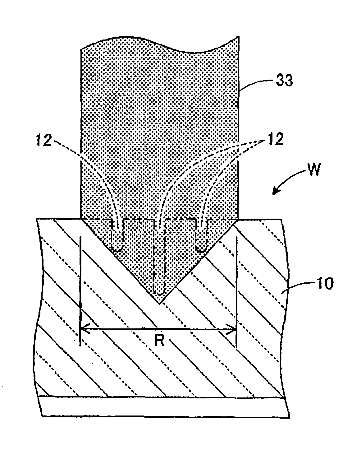
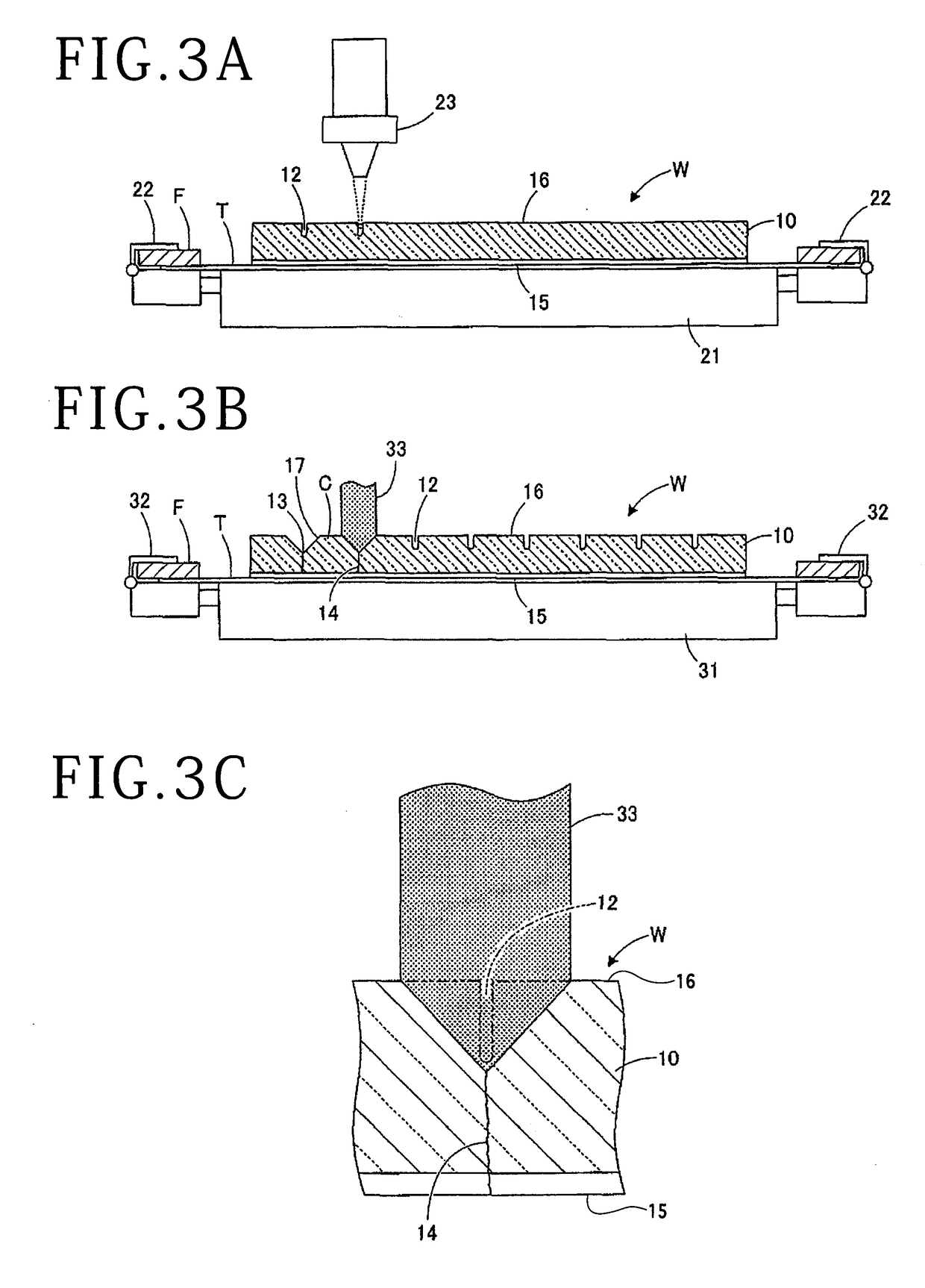
[0032]In the optical device wafer processing method described above, the V groove 13 is formed by the V blade 33 on the optical device wafer W along each division line where the laser processed groove 12 has been formed to reduce the strength of the wafer W. At the same time, the optical device wafer W is divided along each V groove 13. That is, a processing load is applied from the V blade 33 to the optical device wafer W along each laser processed groove 12 in forming the V groove 13, so that excess load is hardly applied to the side surfaces of the V groove 13 and the generation of cracks on the side surfaces of each device chip C can therefore be suppressed. Further, the inclined surfaces 17 of each device chip C can be formed by the side surfaces of each V groove 13 formed on the optical device wafer W, thereby increasing the amount of light to be extracted from each device chip C and accordingly improving the luminance.

[0033]An optical device wafer processing method according...

second embodiment

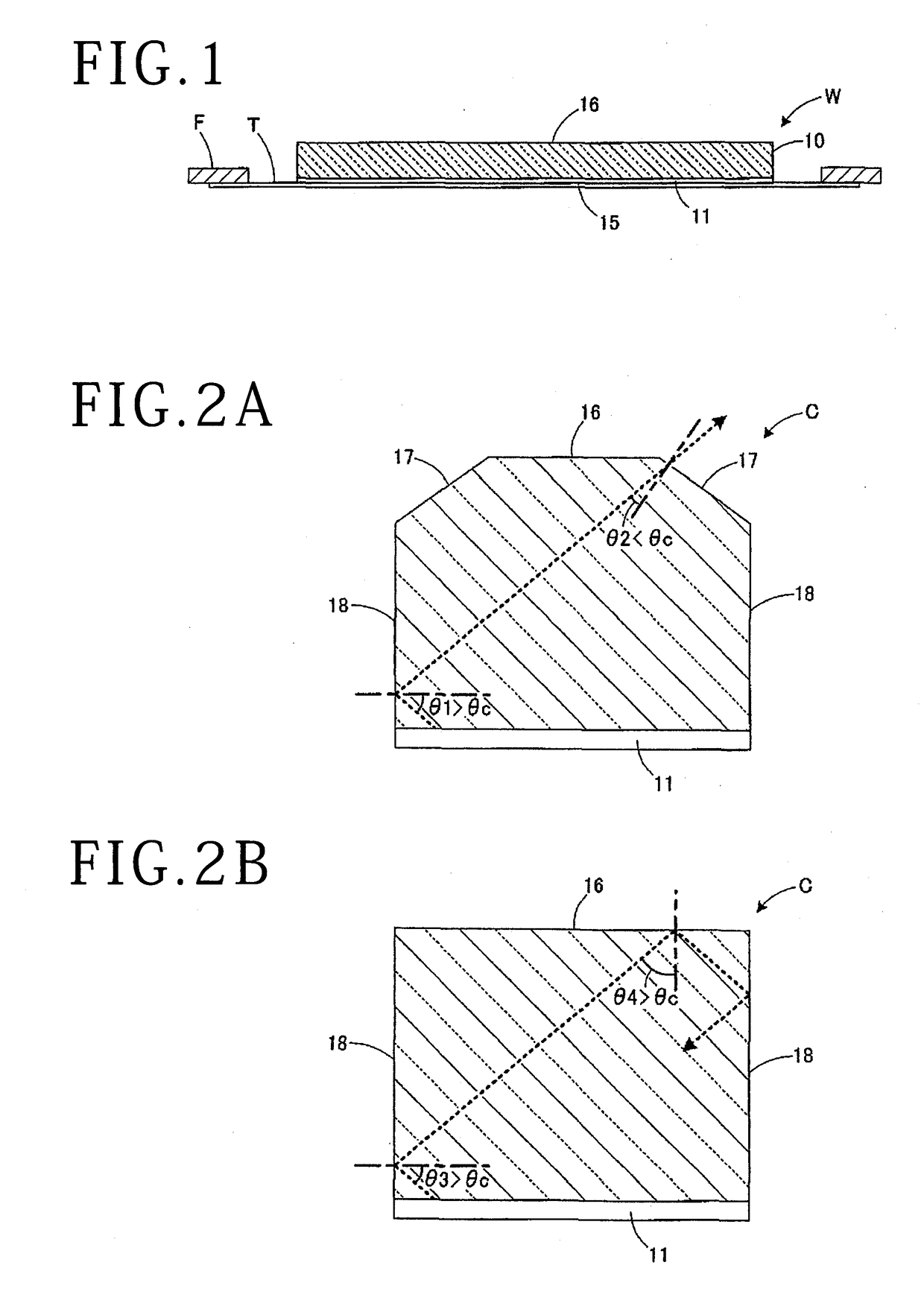
[0039]Accordingly, the inclined surfaces 17 (see FIG. 2A) of each device chip C are formed by the side surfaces of each V groove 13 of the optical device wafer W, thereby improving the light extraction efficiency of each device chip C. Further, since the generation of cracks is suppressed in forming each V groove 13, the quality of each device chip C can be improved. The dividing step may be performed by using any apparatus capable of applying an external force to the optical device wafer W along each V groove 13 to thereby divide the optical device wafer W into the individual device chips C. For example, a tape expander for expanding the support tape T may be used to apply an external force to the optical device wafer W, thereby dividing the optical device wafer W. In the second embodiment, the breaking apparatus as a special apparatus dedicated to division is used to divide the optical device wafer W, so that the optical device wafer W can be divided well and reliably.

[0040]In the...


PUM


Abstract

An optical device wafer processing method for dividing an optical device wafer along a plurality of division lines to obtain a plurality of individual device chips includes applying a laser beam to a wafer substrate along each division line to thereby form a laser processed groove along each division line, and next forming a V groove along each laser processed groove on the optical device wafer by using a cutting blade having a V-shaped tip in the condition where each laser processed groove is removed by the cutting blade. A crack is formed so as to extend from the bottom of each laser processed groove due to a load applied from the cutting blade, thereby dividing the optical device wafer into the individual device chips. The depth of each laser processed groove is set smaller than the depth of cut by the cutting blade.

Description

BACKGROUND OF THE INVENTIONField of the Invention[0001]The present invention relates to an optical device wafer processing method for dividing an optical device wafer along division lines.Description of the Related Art[0002]A functional layer of hexagonal single crystal such as SiC and GaN is formed on a substrate, and this functional layer is partitioned by a plurality of crossing division lines to thereby form a plurality of optical devices such as power devices, light emitting diodes (LEDs), and laser diodes (LDs) on the substrate. Thus, an optical device wafer having the plural optical devices on the front side is obtained. As a method of dividing the optical device wafer along the division lines to obtain a plurality of individual device chips, there has been proposed a method including the steps of applying a pulsed laser beam having an absorption wavelength to the substrate along each division line to thereby form a laser processed groove as a break start point along each div...

Claims


Application Information

Patent Timeline
IPC IPC(8): H01L33/00H01L33/20
CPCH01L33/0079H01L33/20H01L33/32B23K26/364B28D5/0011H01L21/304H01L21/3043H01L33/0095H01L33/005H01L21/78H01L21/76H01L33/0093
Inventor OKAMURA, TAKASHI
Owner DISCO CORP
Why Eureka
Try Eureka