SiC WAFER PRODUCING METHOD

a wafer and production method technology, applied in the direction of crystal growth process, manufacturing tools, after-treatment details, etc., can solve the problem of more economic production of sic wafer from sic ingots, and achieve the effects of reducing the thickness strengthening the sic wafer, and improving the heat dissipation of the sic wafer

Active Publication Date: 2018-08-02
DISCO CORP
View PDF0 Cites 19 Cited by
  • Summary
  • Abstract
  • Description
  • Claims
  • Application Information

AI Technical Summary

Benefits of technology

[0005]However, in separating the SiC wafer from the SiC ingot or in forming devices on the front side of the SiC wafer, the thickness of the SiC wafer to be separated from the SiC ingot is set to approximately 700 to 800 μm, so as to strengthen the SiC wafer. Further, in order to improve heat dissipation in di

Problems solved by technology

Accordingly, there is a problem in producing the

Method used


Image

  • SiC WAFER PRODUCING METHOD
  • SiC WAFER PRODUCING METHOD
  • SiC WAFER PRODUCING METHOD

Examples


Embodiment Construction

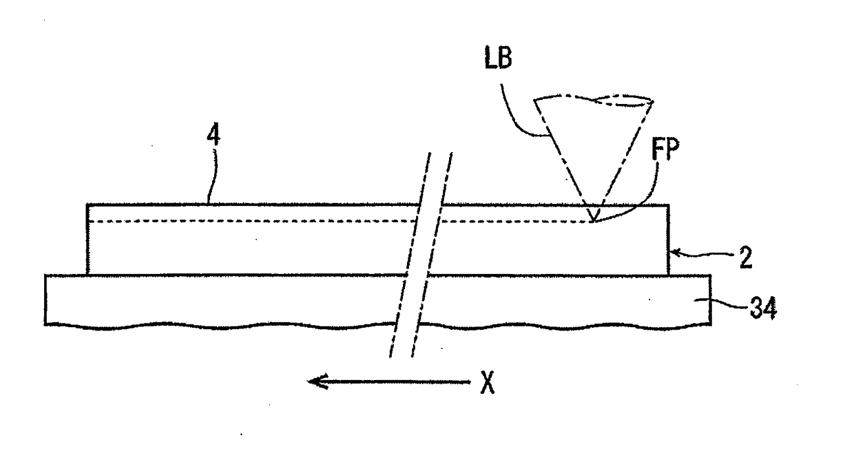
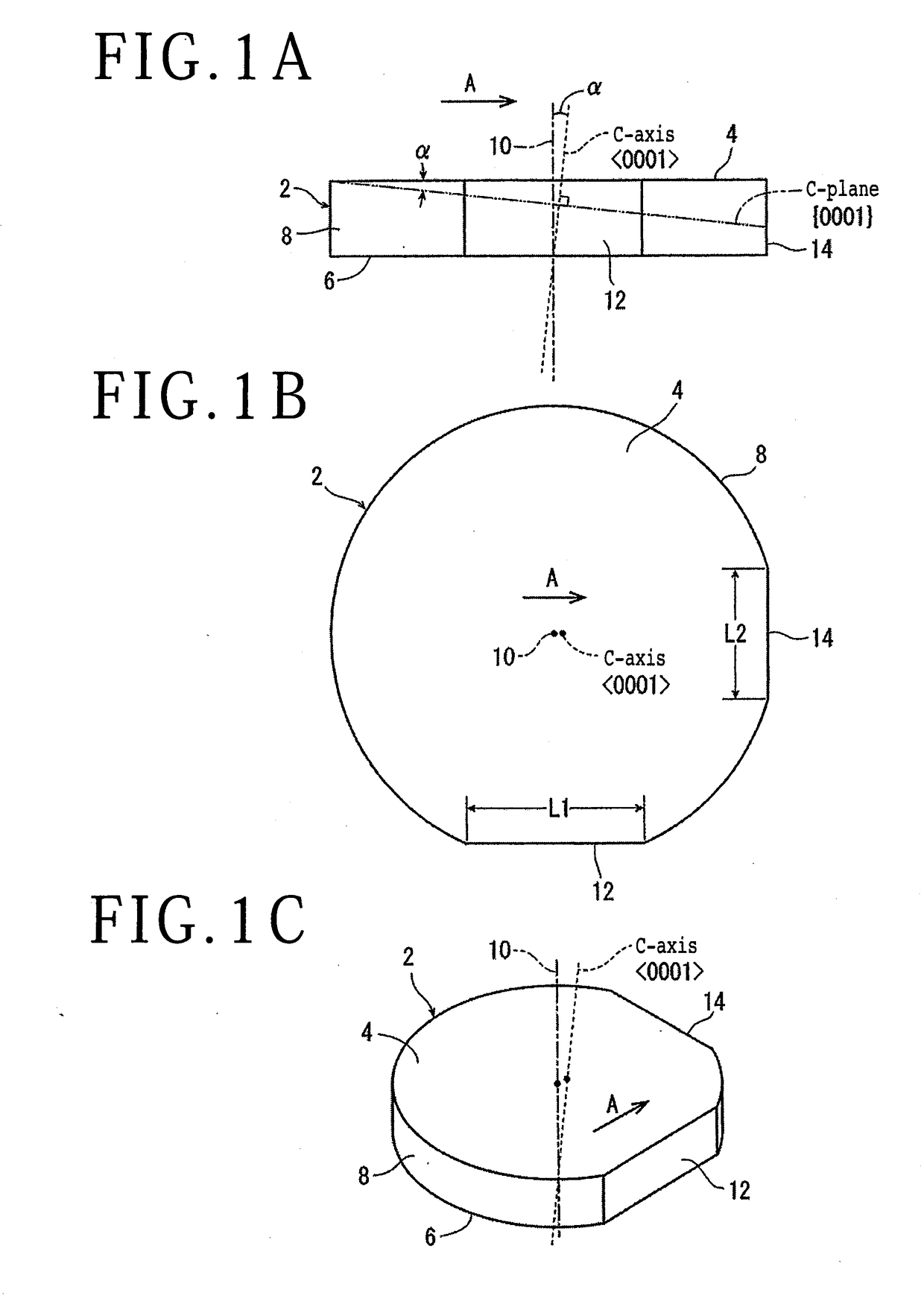
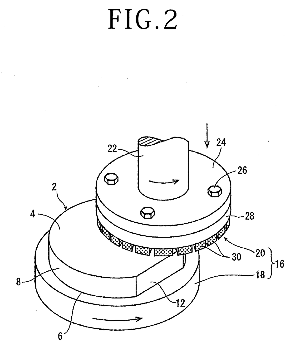
[0028]A preferred embodiment of the wafer producing method according to the present invention will now be described with reference to the drawings. FIGS. 1A to 1C depict a substantially cylindrical, hexagonal single crystal SiC ingot 2 (which will be hereinafter referred to simply as “ingot 2”) as a workpiece to be processed. The ingot 2 has a substantially circular first surface 4, a substantially circular second surface 6 opposite to the first surface 4, a substantially cylindrical surface 8 formed so as to connect the first surface 4 and the second surface 6, a c-axis ( direction) extending from the first surface 4 to the second surface 6, and a c-plane ({0001} plane) perpendicular to the c-axis. In the ingot 2, the c-axis is inclined by an off angle α (e.g., α=1, 3, or 6 degrees) with respect to a normal 10 to the first surface 4. The off angle α is formed between the c-plane and the first surface 4. The direction of formation of the off angle α (i.e., the direction of inclinati...


PUM

PropertyMeasurementUnit
Thicknessaaaaaaaaaa

Abstract

A method for producing a wafer from an ingot of single crystal SiC includes an end surface planarizing step of planarizing an end surface of the ingot, a separation layer forming step of setting a focal point of a laser beam having a transmission wavelength to single crystal SiC inside the ingot at a predetermined depth from the end surface of the ingot, the predetermined depth corresponding to the thickness of the wafer to be produced, and next applying the laser beam to the ingot to thereby form a separation layer for separating the wafer from the ingot, a hard plate providing step of providing a hard plate through an adhesive on the end surface of the ingot in which the separation layer has been formed, and a separating step of separating the wafer with the hard plate from the ingot along the separation layer.

Description

BACKGROUND OF THE INVENTIONField of the Invention[0001]The present invention relates to an SiC wafer producing method for producing an SiC wafer from a single crystal SiC ingot.Description of the Related Art[0002]Various devices such as integrated circuits (ICs), Large Scale Integrations (LSIs), and light emitting diodes (LEDs) are formed by forming a functional layer on the front side of a wafer formed of Si (silicon) or Al2O3 (sapphire) and partitioning this functional layer into a plurality of separate regions along a plurality of division lines. Further, power devices or optical devices such as LEDs are formed by forming a functional layer on the front side of a wafer formed of single crystal SiC (silicon carbide) and partitioning this functional layer into a plurality of separate regions along a plurality of division lines. The division lines of such a wafer having these devices are processed by a processing apparatus such as a cutting apparatus and a laser processing apparatus...

Claims


Application Information

Patent Timeline
IPC IPC(8): H01L21/02H01L29/16H01L21/683H01L21/78B23K26/38B24B7/22
CPCH01L21/02013H01L29/1608H01L21/6836H01L21/78B23K26/38B24B7/228B23K26/402B24B7/16B28D5/0058B28D5/0082B28D5/04C30B33/00B23K26/364H01L21/6835H01L2221/68327C30B29/36C30B33/06H01L33/005
Inventor HIRATA, KAZUYA
Owner DISCO CORP
Why Eureka
Try Eureka