Flexible vertical channel organic thin film transistor and manufacture method thereof

Inactive Publication Date: 2018-08-02
WUHAN CHINA STAR OPTOELECTRONICS TECH CO LTD
View PDF7 Cites 10 Cited by
  • Summary
  • Abstract
  • Description
  • Claims
  • Application Information

AI Technical Summary

Benefits of technology

[0005]An objective of the present invention is to provide a manufacture method of a flexible vertical channel organic thin film transistor, and the manufactured flexible vertical channel organic thin film transistor has a sh

Problems solved by technology

However, the LTPS backplate technology increases the process time, the energy consumption and the cost.
The manufacture technology has difficulty to ensure obtaining the uniform large area thin film.
Then, the pixel driven thereby shows the issue of unstable illumination.
In the meantime, the manufacture process is more complicated.
However, the carrier mobility is lower, and for obtaining the current capable of drivi

Method used


Image

  • Flexible vertical channel organic thin film transistor and manufacture method thereof
  • Flexible vertical channel organic thin film transistor and manufacture method thereof
  • Flexible vertical channel organic thin film transistor and manufacture method thereof

Examples


Example

[0046]For better explaining the technical solution and the effect of the present invention, the present invention will be further described in detail with the specific embodiments.

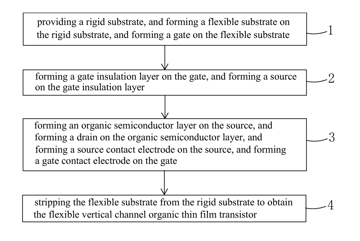
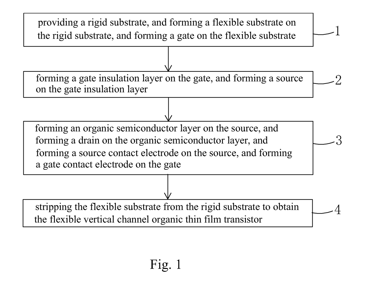
[0047]Please refer to FIG. 1. The present invention first provides a manufacture method of a flexible vertical channel organic thin film transistor, comprising steps of:

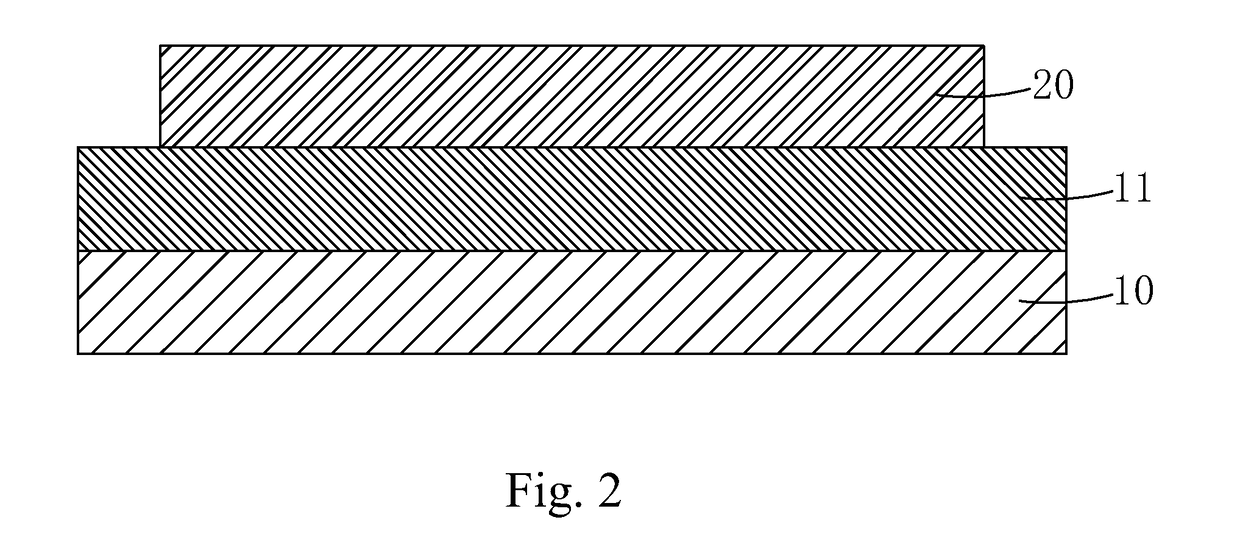
[0048]step 1, as shown in FIG. 1, providing a rigid substrate 10, and forming a flexible substrate 11 on the rigid substrate 10, and forming a gate 20 on the flexible substrate 11.

[0049]Specifically, the rigid substrate 10 is a glass substrate.

[0050]Preferably, the material of the flexible substrate 11 is a polyimide (PI) thin film.

[0051]Specifically, the material of the gate 20 is graphene, and preferably is zero defect graphene.

[0052]Specifically, in step 1, the manufacture method of the gate 20 is: employing a method of chemical vapor deposition (CVD) to deposit a graphene layer on the flexible substrate 11, and then patterning the graph...


PUM


Abstract

Provided is a flexible vertical channel organic thin film transistor and a manufacture method thereof, which change the traditional configuration of the horizontal channel organic TFT and use the vertical channel configuration to tremendously shorten the channel length so that the TFT can obtain the larger source-drain current under the lower drive voltage; by using the flawless, high conductive and high transparent graphene material to manufacture the gate, the electronic performance of the TFT can be better; by using the hexagonal boron nitride material to manufacture the gate insulation layer to interact with the gate made by graphene, the electronic performance of the TFT can be promoted; because both the graphene and the hexagonal boron nitride materials are two dimension atomic layer structure material with better bendability and the channel layer uses the flexible organic semiconductor layer, the bendability of the entire TFT can be significantly promoted.

Description

FIELD OF THE INVENTION[0001]The present invention relates to a display technology field, and more particularly to a flexible vertical channel organic thin film transistor and a manufacture method thereof.BACKGROUND OF THE INVENTION[0002]With the development of display technology, the flat panel device, such as Liquid Crystal Display (LCD) possesses advantages of high image quality, power saving, thin body and wide application scope. Thus, it has been widely applied in various consumer electrical products, such as mobile phone, television, personal digital assistant, digital camera, notebook, laptop, and becomes the major display device.[0003]The Organic Light Emitting Display (OLED) display, which is also named as Organic electroluminescent display, is a new flat panel display device. Because it possesses many outstanding properties of self-illumination, low driving voltage, high luminescence efficiency, short response time, high clarity and contrast, near 180° view angle, wide rang...

Claims


Application Information

Patent Timeline
IPC IPC(8): H01L27/32H01L51/10H01L51/05H01L51/52
CPCH01L27/3274H01L51/102H01L51/0558H01L51/0525H01L51/057H01L51/5206H01L27/3262H01L51/0048H01L29/7827H10K50/00H10K50/80H10K71/00H10K59/1213H10K59/125H10K85/221H10K10/472H10K10/491H10K10/82H10K10/484H10K50/81
Inventor BU, CHENGHAOHU, GUOREN
Owner WUHAN CHINA STAR OPTOELECTRONICS TECH CO LTD
Why Eureka
Try Eureka