Multilayer ceramic capacitor and manufacturing method of multilayer ceramic capacitor

a manufacturing method and multi-layer ceramic technology, applied in the direction of fixed capacitors, stacked capacitors, fixed capacitor details, etc., can solve the problem of not defined donor elements in the dielectric layer

Inactive Publication Date: 2018-08-16
TAIYO YUDEN KK
View PDF16 Cites 5 Cited by
  • Summary
  • Abstract
  • Description
  • Claims
  • Application Information

AI Technical Summary

Benefits of technology

The present invention relates to a multilayer ceramic capacitor and its manufacturing method. The technical effect of this invention is to achieve a preferable life property of the dielectric layer by controlling the position of the donor element in the dielectric layer. The invention provides a multilayer ceramic capacitor and its manufacturing method with a defined donor element concentration in the dielectric layer, which results in a current value at a specific temperature that meets certain requirements. This improves the reliability and performance of the multilayer ceramic capacitor.

Problems solved by technology

However, in the technologies, a position of the donor element in the dielectric layer is not defined.

Method used


Image

  • Multilayer ceramic capacitor and manufacturing method of multilayer ceramic capacitor
  • Multilayer ceramic capacitor and manufacturing method of multilayer ceramic capacitor
  • Multilayer ceramic capacitor and manufacturing method of multilayer ceramic capacitor

Examples


embodiment

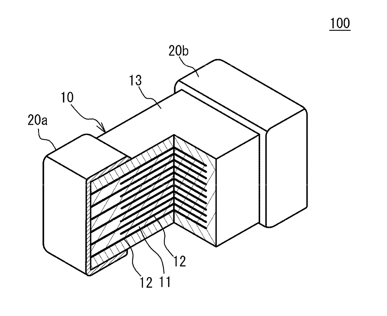
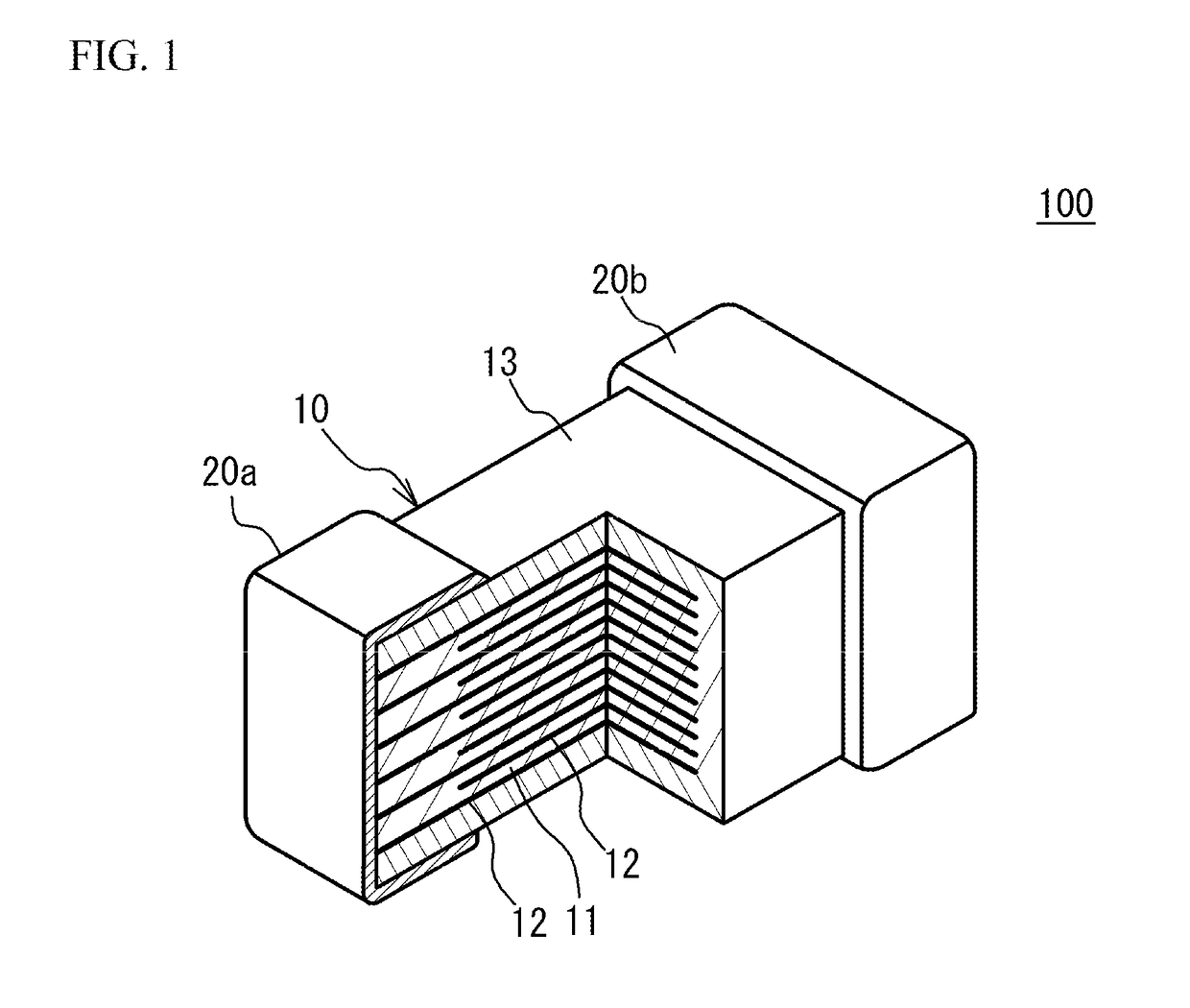
[0015]FIG. 1 illustrates a partial perspective view of a multilayer ceramic capacitor 100 in accordance with an embodiment. As illustrated in FIG. 1, the multilayer ceramic capacitor 100 includes a multilayer chip 10 having a rectangular parallelepiped shape, and a pair of external electrodes 20a and 20b that are respectively provided at two edge faces of the multilayer chip 10 facing each other. In four faces other than the two edge faces of the multilayer chip 10, two faces other than an upper face and a lower face of the multilayer chip 10 in a stacking direction are referred to as side faces. The external electrodes 20a and 20b extend to the upper face, the lower face and the two side faces. However, the external electrodes 20a and 20b are spaced from each other.

[0016]The multilayer chip 10 has a structure designed to have dielectric layers 11 and internal electrode layers 12 alternately stacked. The dielectric layer 11 includes ceramic material acting as a dielectric material. ...

example 1

[0036]In an example 1, barium titanate was used as the main component ceramic of the dielectric layer 11. Mo was used as the donor element. MoO3 was added to the main component ceramic powder so that Mo is 0.2 atm % on a presumption that Ti of the main component ceramic powder is 100 atm %. The resulting main component ceramic powder was sufficiently wet-blended and crushed with a ball mil. Thus, the dielectric material was obtained. An organic binder and a solvent were added to the dielectric material. And dielectric green sheets were made by a doctor blade method. The organic binder was polyvinyl butyral (PVB) resin or the like. The solvent was ethanol, toluene or the like. And a plasticizer and so on were added. Next, the conductive paste for forming the internal electrode layer 12 was made by mixing powder acting as a main component metal of the internal electrode layer 12, a binder, a solvent and an additive as needed. The organic binder and the solvent were different from thos...

example 2

[0037]In an example 2, a main component ceramic powder in which 0.05 atm % of Mo was solid-solved in advance was used as the dielectric material. A Mo source was not added to the main component ceramic powder. Other conditions were the same as those of the example 1.


PUM

PropertyMeasurementUnit
Thicknessaaaaaaaaaa
Diameteraaaaaaaaaa
Diameteraaaaaaaaaa

Abstract

A multilayer ceramic capacitor includes: a multilayer structure in which each of a plurality of ceramic dielectric layers and each of a plurality of internal electrode layers are alternately stacked, wherein: (a current value at 10 V / μm when a direct voltage is applied to the plurality of the ceramic dielectric layers at 125 degrees C.) / (a current value at 10 V / μm when a direct voltage is applied to the plurality of the ceramic dielectric layers at 85 degrees C.) is more than 5 and less than 20; and a donor element concentration in the plurality of ceramic dielectric layers is 0.05 atm % or more and 0.3 atm % or less.

Description

CROSS-REFERENCE TO RELATED APPLICATION[0001]This application is based upon and claims the benefit of priority of the prior Japanese Patent Application No. 2017-027330, filed on Feb. 16, 2017, the entire contents of which are incorporated herein by reference.FIELD[0002]A certain aspect of the present invention relates to a multilayer ceramic capacitor and a manufacturing method of a multilayer ceramic capacitor.BACKGROUND[0003]A thickness of a dielectric layer is being reduced because downsizing and enhancement of a capacitance of a multilayer ceramic capacitor are demanded. As a result, electric field intensity applied to the dielectric layer increases. Thereby, life property of the dielectric layer is degraded. And so, it is proposed that a donor element such as Mo (molybdenum), W (tungsten) or the like is added to a dielectric layer in order to improve life property (for example, see Japanese Patent Application Publications No. 2016-139720 and No. 2016-127120).SUMMARY OF THE INVEN...

Claims


Application Information

Patent Timeline
IPC IPC(8): H01G4/12H01G4/30
CPCH01G4/1209H01G4/30C04B2235/3206C04B2235/3256C04B2235/3251C04B2235/3258B32B2315/02B32B2457/16C04B2235/78C04B2235/3239H01G13/003H01G4/1227H01G4/012
Inventor TANIGUCHI, KATSUYA
Owner TAIYO YUDEN KK
Why Eureka
Try Eureka