Printable Functional Materials For Plastic Electronics Applications

a functional material and plastic electronics technology, applied in the field of printing formulations, can solve the problems of high cost high thickness of screen printing meh-ppv film, and inability to meet the requirements of large-scale device manufacturing, etc., and achieve the effect of low cost device manufacturing at large-scal

Inactive Publication Date: 2018-08-30
ILIT TECH
View PDF7 Cites 2 Cited by
  • Summary
  • Abstract
  • Description
  • Claims
  • Application Information

AI Technical Summary

Benefits of technology

[0034]Advantageously, screen printing of organic or inorganic electronic devices in accordance with embodiments of the present invention offers the possibility of low cost device manufacturing at large scale. Advantageously, embodiments of the present invention allow the production of fully screen printable large area organic light emitting and photovoltaic devices without the requirement for any cleanroom facility.

Problems solved by technology

However, this technique is very time consuming and not suitable for the manufacturing of large area devices.
In addition, print heads used in this technique are expensive and tend to break very easily.
The thickness of the screen printed MEH-PPV film was very high which severely affected the brightness of the fabricated devices.
Furthermore, due to the application of vacuum deposited cathode, this study was unable to provide fully screen printable functional materials for OLED application.
Similarly, due to the incorporation of evaporated metal cathode of a specific work-function, organic solar cells are also not fully screen printable to date at low cost (B. Qi, Z. G. Zhang, J. Wang, Uncovering the role of cathode buffer layer in organic solar cells, Scientific Reports 5, Article number: 7803, Nature, 2015).
In addition, high vapour pressure solvents in the printable compositions make the screen printing very difficult as solvents with high vapour pressure evaporate very quickly during the printing process, causing imperfections.
However, each technique offers a different unique challenge.
In flexography, lithography, and rotogravure, a common problem is the back transfer of solutions due to poor surface compatibility of the ink to the substrate and also shrinkage of the transferred media.

Method used


Image

  • Printable Functional Materials For Plastic Electronics Applications
  • Printable Functional Materials For Plastic Electronics Applications

Examples


example 1

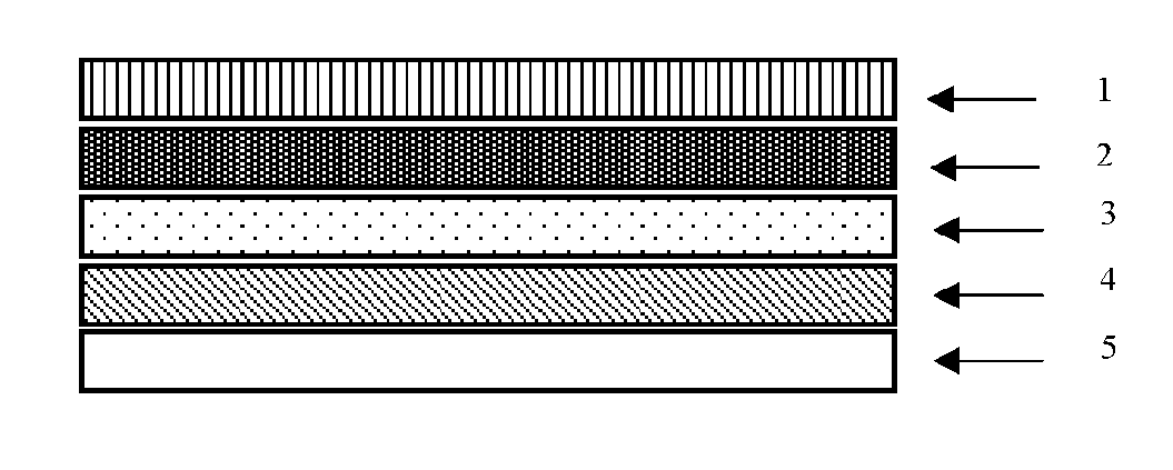
[0044]FIG. 1 shows the device architecture of an OLED that was fabricated on a 2″×2″ sheet of ITO coated PET (150Ω / □) which was cleaned thoroughly using isopropyl alcohol. A hole transport layer (HTL) was then screen printed onto the clean ITO substrate followed by its drying at 120° C. for 15 minutes. A conductive polymer such as PEDOT: PSS was used as a HTL in this case. The emissive layer was made of PFO which was blended with a 2.5 wt % ethyl cellulose dispersion in mesitylene. The amount of PFO in this nanocomposite blend was approximately 1.6% by weight. This nanocomposite blend of PFO and ethyl cellulose was then screen printed onto the HTL coated ITO-PET substrate followed by its curing at 120° C. for 10 minutes. Finally, a cathode material containing 33 wt % Mg and 33 wt % Ag was deposited on the top the PFO based active layer using screen printing technique. The cathode material deposited in this case normally takes 10 minutes to sinter at 120° C.

example 2

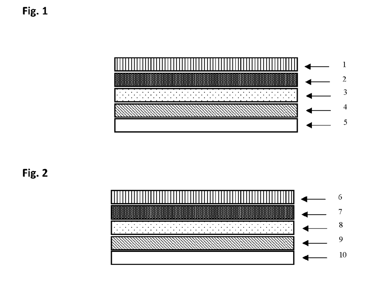
[0045]The same approach as described in Example 1 was used to manufacture a fully screen printable organic solar cell (FIG. 2) on a 1″×1″ flexible substrate based on ITO coated PET (60Ω / □). The substrate was first cleaned using isopropyl alcohol followed by deposition of a thin layer of PEDOT: PSS using screen printing technique. The PEDOT: PSS layer was then annealed at 120° C. for 15 minutes prior to screen printing the P3HT: PCBM / ethyl cellulose based active layer on top. The active layer was also annealed at 120° C. for 15 minutes followed by screen printing the Mg / Ag cathode as a back contact.


PUM

PropertyMeasurementUnit
pressureaaaaaaaaaa
pressureaaaaaaaaaa
pressureaaaaaaaaaa

Abstract

A printable active material formulation comprises a matrix comprising a gelation material and a solvent; and at least one conductive material. A printable cathode formulation comprises a matrix comprising a thermoplastic resin and a solvent; and at least one conductive material. An organic light emitting or photovoltaic device may be manufactured using these formulations, for example by roll-to-roll printing.

Description

FIELD OF THE INVENTION[0001]The present invention relates to a printable formulation, such as an active material or printable cathode formulation, and a method of manufacturing the printable formulation. The present invention further relates to an organic light emitting or photovoltaic device comprising the printable formulation, and a method of manufacturing the same.BACKGROUND OF THE INVENTION[0002]The following discussion is not to be taken as an admission of relevant prior art.[0003]Polymer based electronics or plastic electronics mainly deal with organic materials that display attractive electronic properties that are useful for manufacturing polymer based electronic devices including light emitting diodes and solar cells. Both small molecule organic light emitting diodes (OLEDs) and organic solar cells (OSCs) were first reported by Kodak in 1985 and 1986 respectively, followed by the discovery of polymer OLEDs by Burroughes, Friend, and Bradley in 1988. OLEDs and OSCs possess ...

Claims


Application Information

Patent Timeline
Patent Type & Authority Applications(United States)
IPC IPC(8): H01L51/00H01L51/50H01L51/52H01L51/42H01L51/44
CPCH01L51/0034H01L51/0004H01L51/0022H01L51/5012H01L51/5234H01L51/4253H01L51/442H01L51/0037H01L2251/308Y02E10/549Y02P70/50H10K71/13H10K71/15H10K71/611H10K85/115H10K85/113H10K85/111H10K85/1135H10K85/761H10K30/30H10K50/11H10K50/82H10K2102/331H10K85/10H10K30/82H10K50/828H10K2102/103
Inventor MILES, ANTHONYHUGHES, STEPHEN ROBERTVYAS, NILADRI
Owner ILIT TECH
Why Eureka
Try Eureka