Polarization-doped enhancement mode HEMT

a technology of enhancement mode and polarization, applied in the field of polarization-doped enhancement mode, can solve the problems of limiting the gate voltage swing, affecting the high frequency and switching properties of the device, and affecting so as to achieve the optimization of the horizontal electrical field, the effect of reducing the drift region and improving the breakdown voltage of the devi

Inactive Publication Date: 2018-10-11
UNIV OF ELECTRONICS SCI & TECH OF CHINA
View PDF0 Cites 11 Cited by
  • Summary
  • Abstract
  • Description
  • Claims
  • Application Information

AI Technical Summary

Benefits of technology

[0021]3. In the present invention, 3DEG-3DHG forms the polarization super junction, which assists the depletion of the drift region in a blocking state. The horizontal electrical field is optimized. The breakdown voltage of the device is improved.

Problems solved by technology

One of the important reasons is that the electric field crowding at the gate leads to premature breakdown.
However, the introduction of the field plate increases the parasitic capacitance of the device, which adversely affects the high frequency and switching properties of the device.
Thus, when the device is forward conductive, if the gate voltage is large, leaking current will occur at the gate, which limits the gate voltage swing.
However, recessed gate etching requires precise control of the etch depth and also may cause etch damage.
These methods all realize the enhancement anode by depleting 2DEG under the gate, which will inevitably lead to the contradiction between high threshold voltage and large saturation output current.

Method used


Image

  • Polarization-doped enhancement mode HEMT
  • Polarization-doped enhancement mode HEMT
  • Polarization-doped enhancement mode HEMT

Examples


embodiment 1

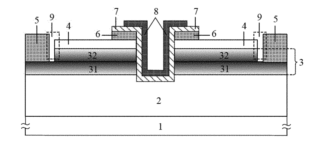
[0033]FIG. 4 shows a polarization-doped enhancement mode HEMT device. The device of the present embodiment comprises:

[0034]substrate layer 1, buffer layer 2, barrier layer 3 and cap layer 4 arranged in an order from bottom to top. The present invention is characterized in that the barrier layer 3 comprises first barrier layer 31 and second barrier layer 32 arranged in an order from bottom to top. The Al composition of the first barrier layer 31 increases progressively from linear or non-linear at the lower surface of x at the upper surface (032 decreases progressively from x (05 which forums Ohmic contact is disposed at the upper surface of the first barrier layer 31. Hole blocking region 9 is disposed between second barrier layer 32, cap layer 4, and metal drain 5. The hole blocking region 9 are formed near the drain end by etching. Metal source 6 is disposed on the upper surface of cap layer 4. A trench insulated gate structure is formed at the side of the metal source 6 that is a...

embodiment 2

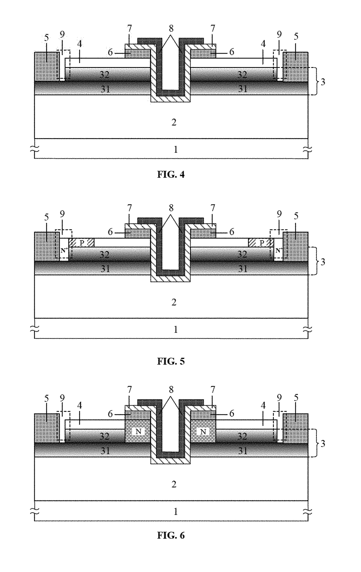
[0036]Compared with Embodiment 1, the device of this Embodiment adopts highly concentrated N-type ion implantation to realize hole blocking region 9 between cap layer 4 and drain 5, so that the hole conductive channel is avoided between the source and the drain. In addition, P-type doping region is formed in part of cap layer 4 which is in contact with hole blocking region 9, so as to avoid the electron leaking path from the source to the drain. Other structures are the same as those of Embodiment 1, as shown in FIG. 5. The ion implantation isolation is easier to realize and has smaller damage on materials. At the same time, NP junction formed between the drain and the source also functions to resist the withstand voltage in the off-state.

embodiment 3

[0037]Compared with Embodiment 1 the device of this Embodiment adopts N-type doping in cap layer 4 and the region of second barrier layer 32 beneath the source. Other structures are the same as those of Embodiment 1, as shown in FIG. 6. On one hand, the N-type doped part beneath the source can make the source metal form a better Ohmic contact with the cap layer. On the other hand, the N-type doping modulates the concentration of the 3DHG, so as to control the threshold voltage.


PUM


Abstract

The present invention belongs to the field of semiconductor technology and relates to a polarization-doped enhancement mode HEMT device. The technical solution of the present invention grows the first barrier layer and the second barrier layer that contain gradient Al composition sequentially on the buffer layer. The gradient trends of the two layers are opposite. The three-dimensional electron gas (3DEG) and the three-dimensional hole gas (3DHG) are induced and generated in the barrier layers due to the inner polarization difference respectively. A trench insulated gate structure is at one side of the source which is away from the metal drain and is in contact with the source. First, since the highly concentrated electrons exist in the entire first barrier layer, the on-state current is improved greatly. Second, the vertical conductive channel between the source and the 3DEG are pinched off by the 3DHG, so as to realize the enhancement mode.

Description

CROSS REFERENCE[0001]This application claims priority to Chinese Patent Application No. 201710222890.4, filed on Apr. 7, 2017 the entire contents of which are incorporated herein by reference.FIELD OF THE INVENTION[0002]The present invention relates to the field of semiconductor technology and more particularly relates to a polarization-doped enhancement mode HEMT.BACKGROUND OF THE INVENTION[0003]GaN-based high electron mobility transistors (HEMTs) have a great prospect in the field of large-current, low-power-consumption, high-frequency and high-voltage switching applications due to high electron saturation speed, high two-dimensional electron gas (2DEG) density and high critical breakdown electric field.[0004]The key of power switching devices is to achieve high breakdown voltage, low power consumption, and high reliability. The critical breakdown electric field of GaN material is ten times that of Si. The breakdown voltage of GaN power device is far lower than its theoretical lim...

Claims


Application Information

Patent Timeline
Patent Type & Authority Applications(United States)
IPC IPC(8): H01L29/15H01L29/06H01L29/207H01L29/423H01L29/78H01L29/20H01L29/10
CPCH01L29/158H01L29/157H01L29/0615H01L29/207H01L29/7788H01L29/7827H01L29/2003H01L29/1054H01L29/4236H01L29/0634H01L29/0684H01L29/205H01L29/42316H01L29/778
Inventor LUO, XIAORONGPENG, FUYANG, CHAOWEI, JIEDENG, SIYUOUYANG, DONGFAZHANG, BO
Owner UNIV OF ELECTRONICS SCI & TECH OF CHINA
Why Eureka
Try Eureka