Methods and systems for microelectronic packaging

a technology of microelectronics and packaging, applied in the field of methods, can solve the problems of limited passive packaging of silicon photonics devices, slow and high cost, and optical losses, and achieve the effect of improving the geometrical uniformity of the optical waveguide structure and reducing the optical gap

Active Publication Date: 2018-10-18
AEPONYX +1
View PDF2 Cites 7 Cited by
  • Summary
  • Abstract
  • Description
  • Claims
  • Application Information

AI Technical Summary

Benefits of technology

[0044]According to an embodiment of the invention there is provided a device comprising an optical waveguide structure can be manipulated to reduce an optical gap between the optical waveguide structure and another optical waveguide structure mounted to at least one of a common carrier with the optical waveguide structure and the optical waveguide structure.
[0045]According to an embodiment of the invention there is provided a device employing at least one of a U-shaped and S-shaped waveguide to improve geometrical uniformity of the optical waveguide structure along the light propagation axis while it is being extended or compressed under the action of a MEMS based micro-positioner.

Problems solved by technology

However, to date, the packaging of photonic integrated circuits to support edge coupling has been restricted to active assembly and thus slow and very expensive as requiring light to perform the alignment.
The passive packaging of silicon photonics devices has thus far been restricted to applications where higher optical losses can be tolerated.
Even with the most innovative waveguide tapers, inverse tapers and mode (spot) size converters to perform mode field conversion and mode field diameter matching, it has been impossible up to now to perform the passive packaging of telecom grade photonic integrated circuits.

Method used


Image

  • Methods and systems for microelectronic packaging
  • Methods and systems for microelectronic packaging
  • Methods and systems for microelectronic packaging

Examples


Embodiment Construction

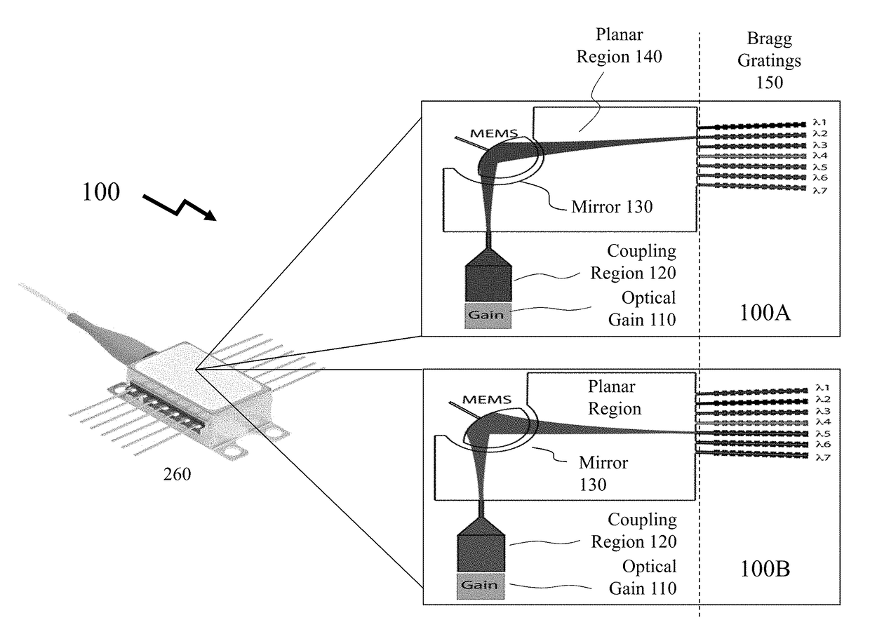
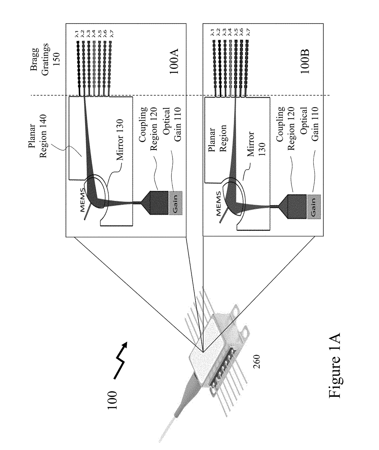
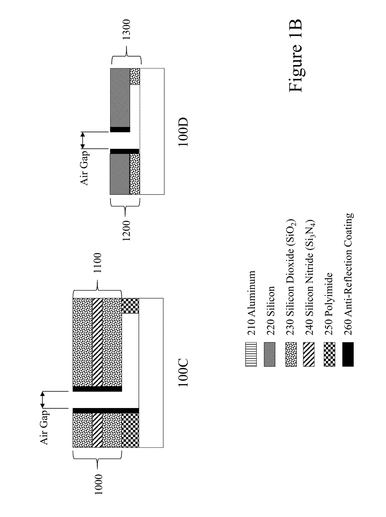
[0107]The present invention is directed to microelectromechanical systems (MEMS) and more particular to designs for optical component packaging and optical coupling employing MEMS devices as part of their design and / or for alignment.

[0108]The ensuing description provides exemplary embodiment(s) only, and is not intended to limit the scope, applicability or configuration of the disclosure. Rather, the ensuing description of the exemplary embodiment(s) will provide those skilled in the art with an enabling description for implementing an exemplary embodiment. It being understood that various changes may be made in the function and arrangement of elements without departing from the spirit and scope as set forth in the appended claims.

[0109]Wavelength Tunable Optical Source

[0110]Wavelength tunable optical sources and / or receivers have significant benefit in the provisioning of transmitters, receivers, and transceivers within todays optical communication networks and evolving requirement...


PUM


Abstract

Hybrid optical integration places very strict manufacturing tolerances and performance requirements upon the multiple elements to exploit passive alignment techniques as well as having additional processing requirements. Alternatively, active alignment and soldering / fixing where feasible is also complex and time consuming with 3, 4, or 6-axis control of each element. However, microelectromechanical (MEMS) systems can sense, control, and activate mechanical processes on the micro scale. Beneficially, therefore the inventors combine silicon MEMS based micro-actuators with silicon CMOS control and drive circuits in order to provide alignment of elements within a silicon optical circuit either with respect to each other or with other optical elements hybridly integrated such as compound semiconductor elements. Such inventive MEMS based circuits may be either maintained as active during deployment or powered off once the alignment has been “locked” through an attachment / retention / latching process.

Description

CROSS-REFERENCE TO RELATED APPLICATIONS[0001]This patent application claims the benefit of priority as a 371 National Phase Entry of Patent Cooperation Treaty Application PCT / CA2015 / 000,466 filed on Aug. 17, 2015 entitled “Methods and Systems for Microelectromechanical Packaging” which itself claims the benefit of priority from U.S. Provisional Patent Application 62 / 037,655 filed on Aug. 15, 2014 entitled “Methods and Systems for Microelectromechanical Packaging.”FIELD OF THE INVENTION[0002]This invention relates to microelectromechanical systems (MEMS) and more particular to designs for optical component packaging and optical coupling employing MEMS devices as part of their design and / or for alignment.BACKGROUND OF THE INVENTION[0003]Silicon Photonics is a promising technology for reducing the cost structure of various optical components by leveraging the economies of scale of the microelectronics industry. In the same way as silicon CMOS circuits can be packaged using multiple die...

Claims


Application Information

Patent Timeline
Patent Type & Authority Applications(United States)
IPC IPC(8): G02B6/35B81B5/00G02B6/124
CPCG02B6/3518B81B5/00G02B6/3596G02B6/357G02B6/124B81B2201/042B81B2201/033G02B6/1228G02B6/4214G02B6/00G02B6/12004G02B2006/12061G02B2006/12078G02B2006/12085G02B2006/12104G02B2006/12107G02B2006/12121G02B2006/12145
Inventor MENARD, FRANCOISNABKI, FREDERICMENARD, MICHA LBERARD, MARTIN
Owner AEPONYX
Why Eureka
Try Eureka