Managed Substrate Effects for Stabilized SOI FETs

a stabilized substrate and substrate technology, applied in the field of electromechanical circuits, can solve the problems of complex switching and control, difficulty in optimizing operational parameters, and acute rf design, and achieve the effect of eliminating or managing accumulated charge and eliminating or mitigating the effects of such accumulated charg

Active Publication Date: 2018-11-22
PSEMI CORP
View PDF3 Cites 44 Cited by
  • Summary
  • Abstract
  • Description
  • Claims
  • Application Information

AI Technical Summary

Benefits of technology

[0028]The invention encompasses several types of modifications in selected regions to silicon-on-insulator (SOI) substrates having a trap rich layer, and methods for making such modifications. The modified regions eliminate or manage accumulated charge that would otherwise arise because of the interaction of the underlying trap rich layer and active layer devices undergoing transient changes of state, thereby eliminating or mitigating the effects of such accumulated charge on non-RF integrated circuitry fabricated on such substrates.

Problems solved by technology

Importantly, in modern transceivers, there are often more than one receiver path Rx and transmitter path Tx—for example, to accommodate multiple frequencies and / or signaling modalities—so switching and control becomes more complex.
A challenge with electronic circuit design in general is that ideal components do not exist, particularly when dealing with RF signals.
As another example, a significant problem with RF circuit design is eliminating or controlling unwanted cross-effects (“cross-talk”) and self-effects, such as parasitic capacitances and inductances, undesired signal coupling, performance changes due to environment temperature changes as well as self-heating, and others.
The problems of RF design become more acute when embodying RF circuits as ICs, where components materials, circuit juxtaposition, and power constraints add to the difficulties of optimizing operational parameters for all components.
As one example, FETs are inherently designed to operate with fields, but fields do not have distinct edges and often cause cross-effects and self-effects.
A distinct challenge of RF circuit design is that optimization for some circuitry may adversely affect optimization of other circuitry.
Although high resistivity substrates alone are capable of reducing substrate loss when used in SOI IC structures, they are highly susceptible to another phenomenon called parasitic surface conduction.
Therefore, this effect can also lead to signal-degrading cross-talk in RF communication circuits.
However, the improved performance of SOI-based RF circuitry formed in the active layer 408 above the trap rich layer 404 can adversely affect desired operational characteristics of non-RF circuitry formed in the active layer 408 above the trap rich layer 404, such as switches and bias circuits.
Transitioning from a standby mode to an active mode introduces transient effects, especially in bias circuits, which can take a long time to settle out.
However, many RF and analog performance requirements typically do not allow a lot of recovery (“buffer”) time.
The accumulated charge may cause adverse effects, such as opening of parasitic transistors in the structure and causing OFF-state leakages (resulting in higher current consumption), and also causes a history effect, which is the dependence of the threshold voltage VTH of a FET on the previous states of the FET.
Regardless of source, accumulated charge can take a long time to equilibrate (e.g., >4 mS), and can affect the intrinsic properties of a FET device (e.g., the threshold voltage of the device, VTH).
Thus, turning most or all switch FETs OFF to achieve a standby mode power level specification—as in the WiFi example above—results in accumulated charge in or near the trap rich layer 404 which takes time to dissipate when the FETs are turned back ON to the point of stable gain; that time may exceed a required sleep-to-active transition specification.
Anything that affects the operating point of a FET (e.g., VTH, biasing, current IDS, etc.) generally adversely impacts the performance of circuits based on such devices, such as the gain stability of an amplifier circuit.
Under such conditions, turning a FET completely OFF and then getting it to turn ON and be completely stable immediately is quite challenging.
Even providing substrate contacts (S-contacts) to mitigate accumulated charges of various types, as taught in U.S. patent application Ser. No. 14 / 964,412 referenced above, does not fully mitigate the problem during operation (even if the contacts are ohmic), due to the high resistivity of the substrate 402 restricting the flow of charge.
Moreover, anything coupling to the substrate 402 may change its potential, thereby affecting nearby FET devices.
However, such circuit specific solutions are generally inadequate as a general solution.

Method used


Image

  • Managed Substrate Effects for Stabilized SOI FETs
  • Managed Substrate Effects for Stabilized SOI FETs
  • Managed Substrate Effects for Stabilized SOI FETs

Examples


first embodiment

[0073]In a first embodiment, a trap rich layer is selectively formed on a high resistivity substrate.

[0074]FIG. 5A is a block diagram showing an in-process step in the manufacture of an SOI wafer 500 having a high resistivity substrate 402. In this example, a mask is used to define a trap rich region 502 on the high resistivity substrate 402 (shown truncated vertically, the actual proportions would more typically resemble FIG. 4). The trap rich region 502 is otherwise formed on the high resistivity substrate 402 in a conventional manner in a pattern defined by the mask.

[0075]The stepped area adjacent the trap rich region 502 is a “non-TR region”504. In some embodiments, a filler material 508, such as BOX, may be deposited within the non-TR region 504 adjacent the trap rich region 502 to provide a flatter surface. As should be apparent, more than one trap rich region 502 and more than one non-TR region 504 can be formed in different areas of an SOI wafer 500. When using a filler mate...

second embodiment

[0082]In a second embodiment, characteristics of a trap rich layer are modified before formation of a BOX insulator layer.

[0083]FIG. 6A is a block diagram showing an in-process step in the manufacture of an SOI wafer 600 having a high resistivity substrate 402 and a trap rich layer 404. In this example, the trap rich layer 404 has already been formed on the high resistivity substrate 402 (shown truncated vertically, the actual proportions would more typically resemble FIG. 4).

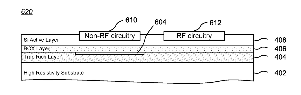
[0084]Before forming a BOX insulator layer 406 over the trap rich layer 404, a modification is made to regions of the trap rich layer 404 that would underlie one or more FETs that otherwise would be adversely affected by accumulated charge resulting from the interaction of the trap rich layer 404 and active layer devices undergoing transient changes of state. More specifically, a surface modification step 602 is applied to implant or diffuse a selected dopant into the material of selected areas of the trap rich...

third embodiment

[0091]In a third embodiment, characteristics of a trap rich layer are modified after formation of a BOX insulator layer (and optionally after formation of an active layer).

[0092]FIG. 7A is a block diagram showing an in-process step in the manufacture of an SOI wafer 700 having a high resistivity substrate 402, a trap rich layer 404, and a BOX insulator layer 406. In this example, the trap rich layer 404 and the BOX insulator layer 406 have already been formed on the high resistivity substrate 402 (again, shown truncated vertically, the actual proportions would more typically resemble FIG. 4).

[0093]After forming the BOX insulator layer 406 over the trap rich layer 404, a modification is made to regions of the trap rich layer 404 that would underlie one or more FETs that otherwise would be adversely affected by accumulated charge resulting from the interaction of the trap rich layer 404 and active layer devices undergoing transient changes of state. More specifically, a surface modifi...


PUM


Abstract

Modified silicon-on-insulator (SOI) substrates having a trap rich layer, and methods for making such modifications. The modified regions eliminate or manage accumulated charge that would otherwise arise because of the interaction of the underlying trap rich layer and active layer devices undergoing transient changes of state, thereby eliminating or mitigating the effects of such accumulated charge on non-RF integrated circuitry fabricated on such substrates. Embodiments retain the beneficial characteristics of SOI substrates with a trap rich layer for RF circuitry requiring high linearity, such as RF switches, while avoiding the problems of a trap rich layer for circuitry that is sensitive to accumulated charge effects caused by the presence of the trap rich layer, such as non-RF analog circuitry and amplifiers (including power amplifiers and low noise amplifiers).

Description

CROSS-REFERENCE TO RELATED APPLICATIONS[0001]This application may be related to U.S. patent application Ser. No. ______ , filed May 19, 2017, entitled “Transient Stabilized SOI FETs” (Attorney Docket No. PER-231-PAP), to U.S. patent application Ser. No. 14 / 964,412, filed Dec. 9, 2015, entitled “S-Contact for SOI”, to U.S. patent application Ser. No. 15 / 385,618, filed Dec. 20, 2016, entitled “Systems, Methods and Apparatus for Enabling High Voltage Circuits”, and to U.S. patent application Ser. No. 15 / 268,297, filed Sep. 16, 2016, entitled “Standby Voltage Condition for Fast RF Amplifier Bias Recovery”, all assigned to the assignee of the present invention and hereby incorporated by reference.BACKGROUND(1) Technical Field[0002]The invention relates to electronic circuits, and more particularly to radio frequency circuitry fabricated with silicon-on-insulator technology.(2) Background[0003]Modern radio frequency (RF) transceivers have become ubiquitous, with manifestations found in ce...

Claims


Application Information

Patent Timeline
Patent Type & Authority Applications(United States)
IPC IPC(8): H01L21/02H01L21/8234H01L21/762H01L21/322H01L21/265H01L29/06
CPCH01L21/02658H01L21/823481H01L21/7624H01L21/3226H01L21/265H01L29/0649H01L27/1218H01L29/78603H01L27/1203H01L21/76251H01L21/2652
Inventor ENGLEKIRK, ROBERT MARKBARGROFF, KEITHMURPHY, CHRISTOPHER C.RANTA, TERO TAPIOWILLARD, SIMON EDWARD
Owner PSEMI CORP
Why Eureka
Try Eureka