Method for manufacturing semiconductor memory device

a semiconductor memory and manufacturing method technology, applied in the direction of semiconductor memory devices, basic electric elements, electrical appliances, etc., can solve the problems of structure and the inability to achieve the effect of dual work function gates, and achieve the effect of improving the performance of the semiconductor memory devi

Active Publication Date: 2018-11-29
WINBOND ELECTRONICS CORP
View PDF14 Cites 2 Cited by
  • Summary
  • Abstract
  • Description
  • Claims
  • Application Information

AI Technical Summary

Benefits of technology

[0005]The invention is directed to a method for manufacturing a semiconductor memory device, which is adapted to combine a tr...

Problems solved by technology

However, when N-type gate electrodes and P-type gate electrodes are respectively formed on the periphery region by using a lithography process and an ion implantation process, a subsequent thermal proc...

Method used


Image

  • Method for manufacturing semiconductor memory device
  • Method for manufacturing semiconductor memory device
  • Method for manufacturing semiconductor memory device

Examples


Embodiment Construction

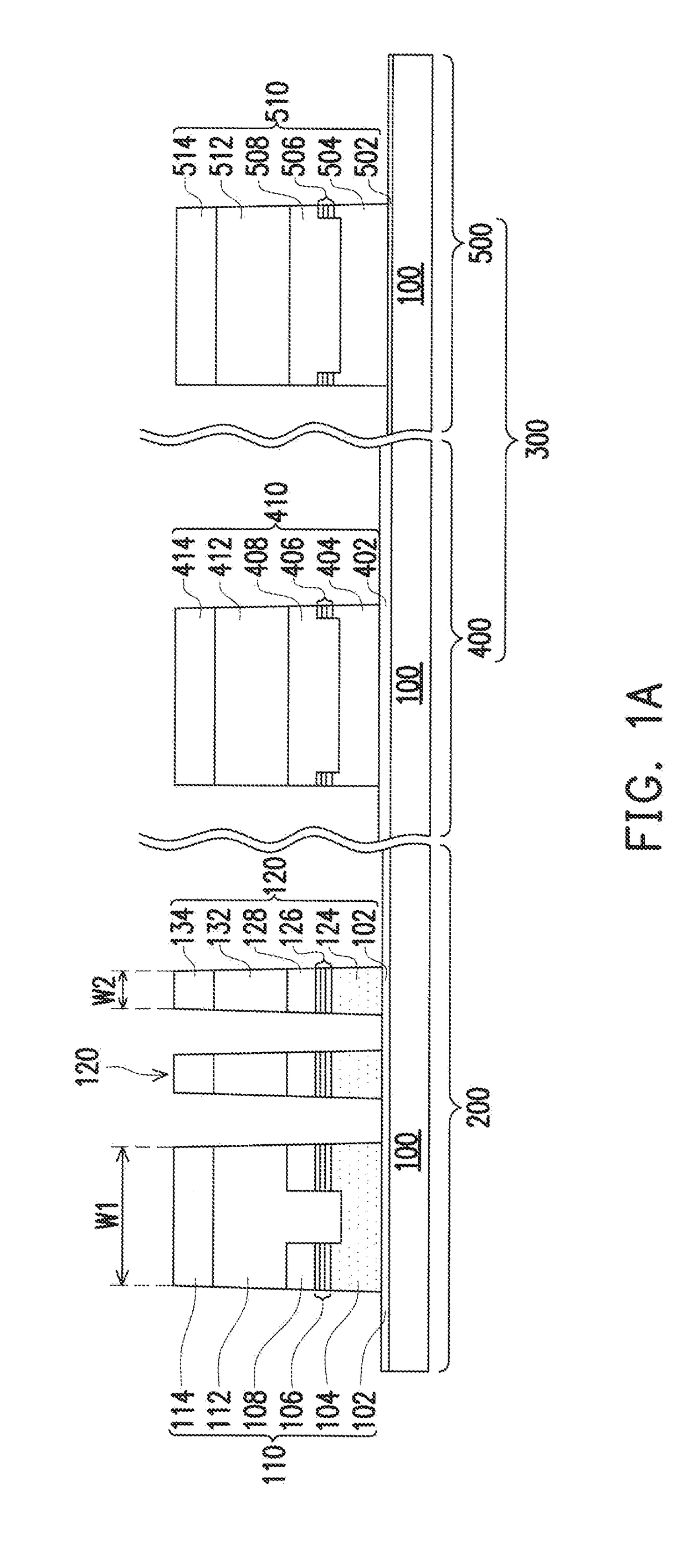
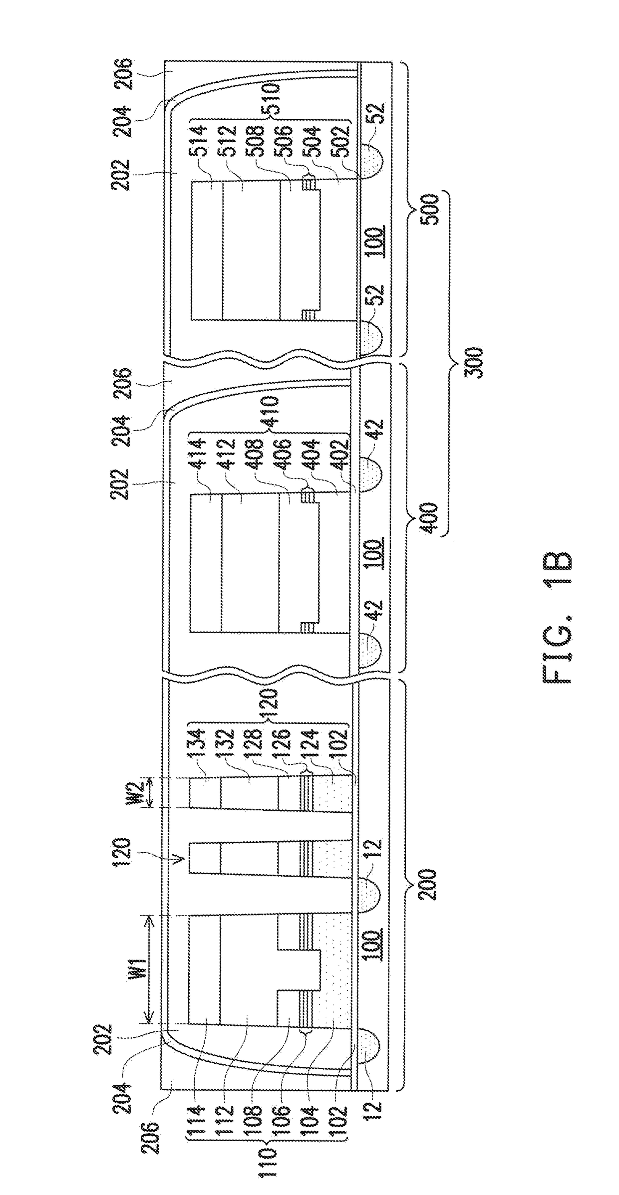
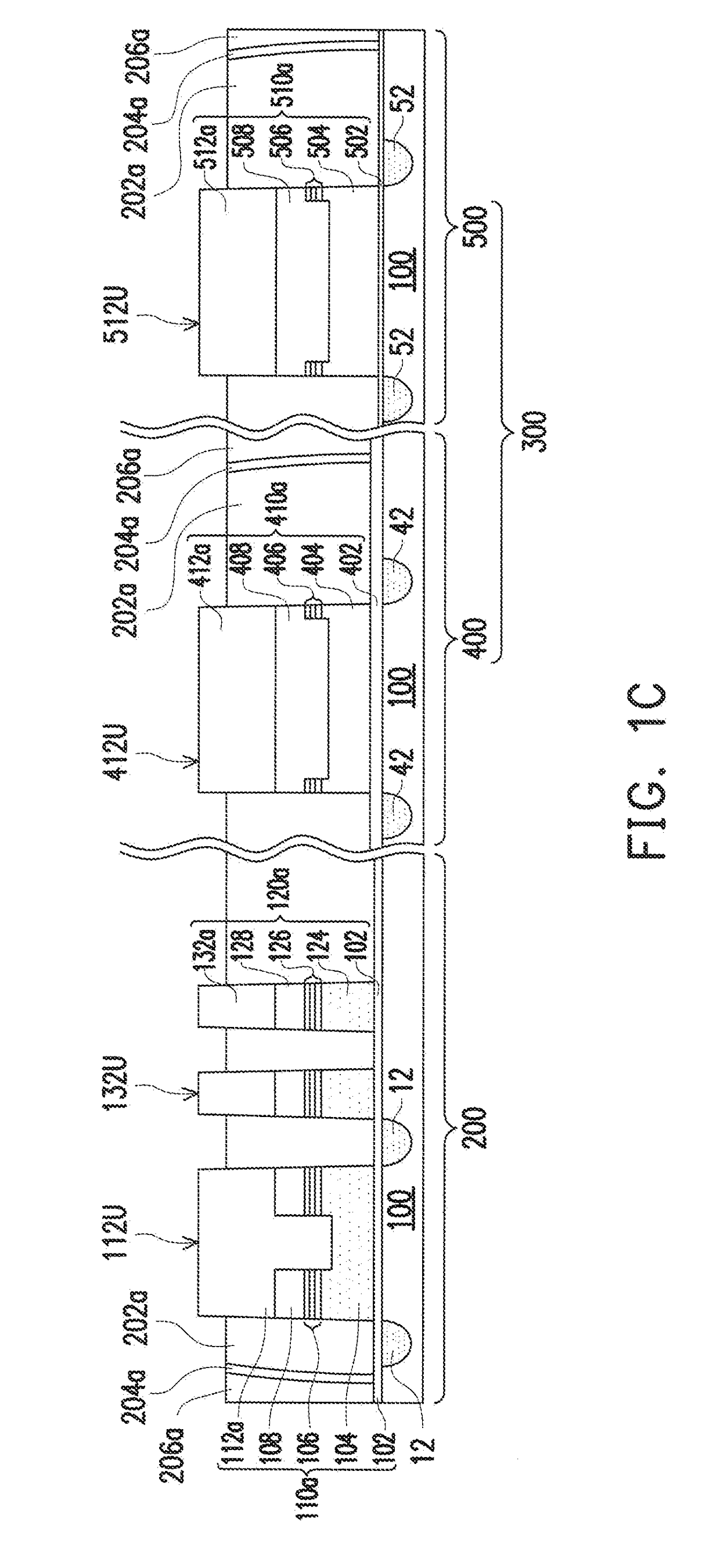
[0011]Referring to the drawings of the invention for a further understanding of the invention. However, the invention can be embodied in various forms, and is not limited to the embodiments provided below. Moreover, the thickness of the layers and regions in the drawings is enlarged for clarity's sake. Wherever possible, the same reference numbers are used in the drawings and the description to refer to the same or like parts, and description thereof are not repeated.

[0012]In the following embodiments, a first conductive type and a second conductive type are different conductive types. Namely, when the first conductivity type is an N-type, the second conductivity type is a P-type; and when the first conductivity type is the P-type, the second conductivity type is the N-type. In the present embodiment, the first conductivity type is, for example, the N-type, and the second conductivity type is, for example, the P-type, though the invention is not limited thereto. The P-type dopant is...


PUM


Abstract

A method for manufacturing a semiconductor memory device including following steps is provided. A substrate having a first region, a second region, and a third region is provided. A first stack structure is formed on the first region. A second stack structure is formed on the second region. A third stack structure is formed on the third region. A first mask layer is formed on the substrate to cover the third stack structure. A first ion implantation process is performed, so that a second floating gate and a second control gate in the second stack structure are changed to a first conductive type. A second mask layer formed on the substrate to cover the first and second stack structures. A second ion implantation process is performed, so that a third floating gate and a third control gate in the third stack structure are changed as a second conductive type.

Description

CROSS-REFERENCE TO RELATED APPLICATION[0001]This application claims the priority benefit of China application serial no. 201710383671.4, filed on May 26, 2017. The entirety of the above-mentioned patent application is hereby incorporated by reference herein and made a part of this specification.BACKGROUND OF THE INVENTIONField of the Invention[0002]The invention relates to a method for manufacturing a semiconductor device, and particularly relates to a method for manufacturing a semiconductor memory device.Description of Related Art[0003]Along with development of technology, in order to meet the demand for reducing cost and simplifying steps of a manufacturing process of a memory device, it has become a trend to integrate elements on a cell region and a periphery region in a single chip. Based on different functions required by the memory device, transistors with different functions are respectively formed in the cell region and the periphery region.[0004]Generally, the transistors ...

Claims


Application Information

Patent Timeline
IPC IPC(8): H01L27/11521H01L27/11529H01L27/11546
CPCH01L27/11521H01L27/11529H01L27/11546H10B41/42H10B41/20H10B41/30H10B41/44H10B41/41H10B41/46H10B41/35H10B41/47H10B41/48H01L29/49H10B41/49
Inventor YANG, CHENG-TACHIANG, LU-PING
Owner WINBOND ELECTRONICS CORP
Why Eureka
Try Eureka