3-Dimensional NOR Memory Array Architecture and Methods for Fabrication Thereof

a technology of memory arrays and layers, applied in semiconductor devices, semiconductor/solid-state device details, instruments, etc., can solve the problems of difficult etching in 3 and undesirable removal of masking layers or layers before etching target materials, and increase the difficulty of etch selectivity, etc., to achieve low cost, mechanical stability, and low resistance metal interconnections

Active Publication Date: 2018-12-20
SUNRISE MEMORY CORP
View PDF0 Cites 59 Cited by
  • Summary
  • Abstract
  • Description
  • Claims
  • Application Information

AI Technical Summary

Benefits of technology

[0007]The present invention addresses obtaining low cost, low resistance metal interconnects and mechanical stability in a high aspect ratio structure. According to the various embodiments disclosed herein, the present invention provides a replacement metal process, which defers the need for a metal etching step in the fabrication process until after all patterned photoresist is no longer present. Under this process, the conductive sublayers may be both thick and numerous. The present invention also provides for a strut structure which facilitates etching steps on high aspect ratio structures, which enhances mechanical stability in a high aspect ratio memory stack.

Problems solved by technology

Conductive sublayers having a metal (e.g., tungsten) that can withstand the subsequent elevated temperature processing (>500° C.) are difficult to etch in 3-D memory structures because of etch selectivity.
It would be undesirable that the masking layer or layers are completely removed before etching of the target material is complete.)
Etch selectivity becomes an even greater problem as each metal sublayer becomes thicker, as a greater number of metal sublayers are present in the stack (e.g. metal shunt sublayers are provided in both source and drain sublayers), and as more memory layers (e.g., 8 or 16 layers of active strips) are provided.
Another problem encountered in fabrication of these memory structures is their mechanical stability, due to their high aspect ratios.
It has been shown that a semiconductor structure with a high aspect ratio can be mechanically unstable, so that the structure leand or even topples completely during the fabrication process.

Method used


Image

  • 3-Dimensional NOR Memory Array Architecture and Methods for Fabrication Thereof
  • 3-Dimensional NOR Memory Array Architecture and Methods for Fabrication Thereof
  • 3-Dimensional NOR Memory Array Architecture and Methods for Fabrication Thereof

Examples


embodiment 1

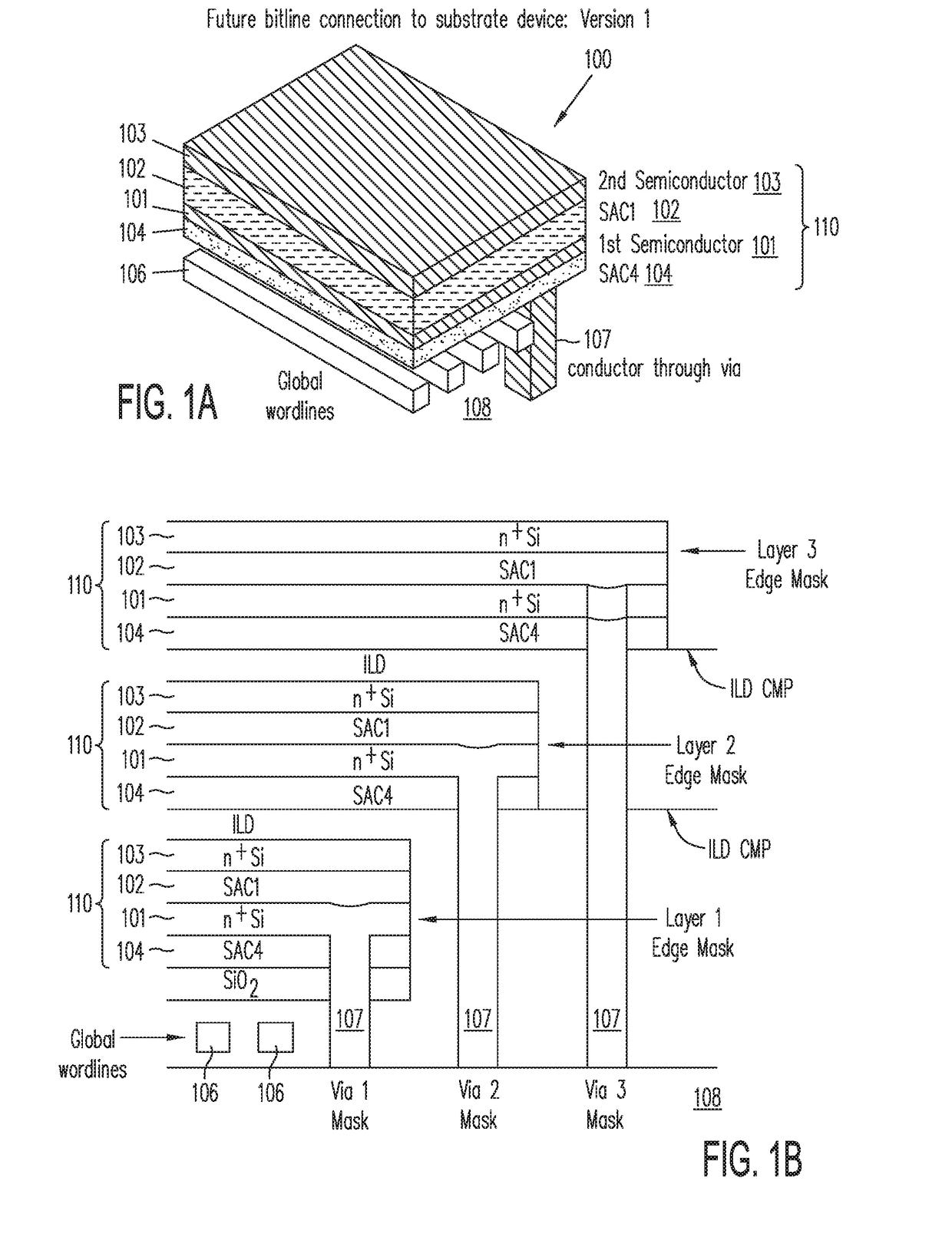
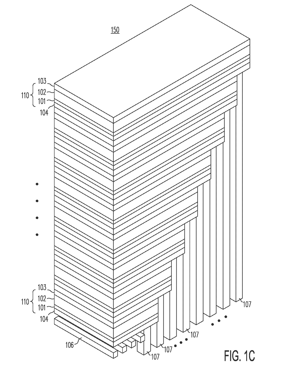
[0084]In this embodiment, tall memory structures with large aspect ratios are achieved using reinforcing struts. The high aspect ratio structures are created after the precursor structures are stabilized by a system of strut structures, and one or more sacrificial layers (“SAC4 sublayers”) are removed by one or more etching steps into the exposed sidewalls of trenches through the NIN stack.

[0085]FIG. 2A shows a cross-sectional schematic of various material layers in memory structure 500, according to one embodiment of the present invention. In FIG. 2A, active layers 502-0 to 502-7 each include drain sublayer 523, source sublayer 521 and sacrificial material 1 (“SAC1”) sublayer 522 (to be subsequently wholly or partially replaced by a channel material sublayer). In addition, sacrificial material 4 (SAC4) sublayer 524 is provided, to be subsequently replaced by a conductive sublayer which electrically contacts drain sublayer 523 substantially throughout its entire length. FIG. 2B show...

embodiment 2

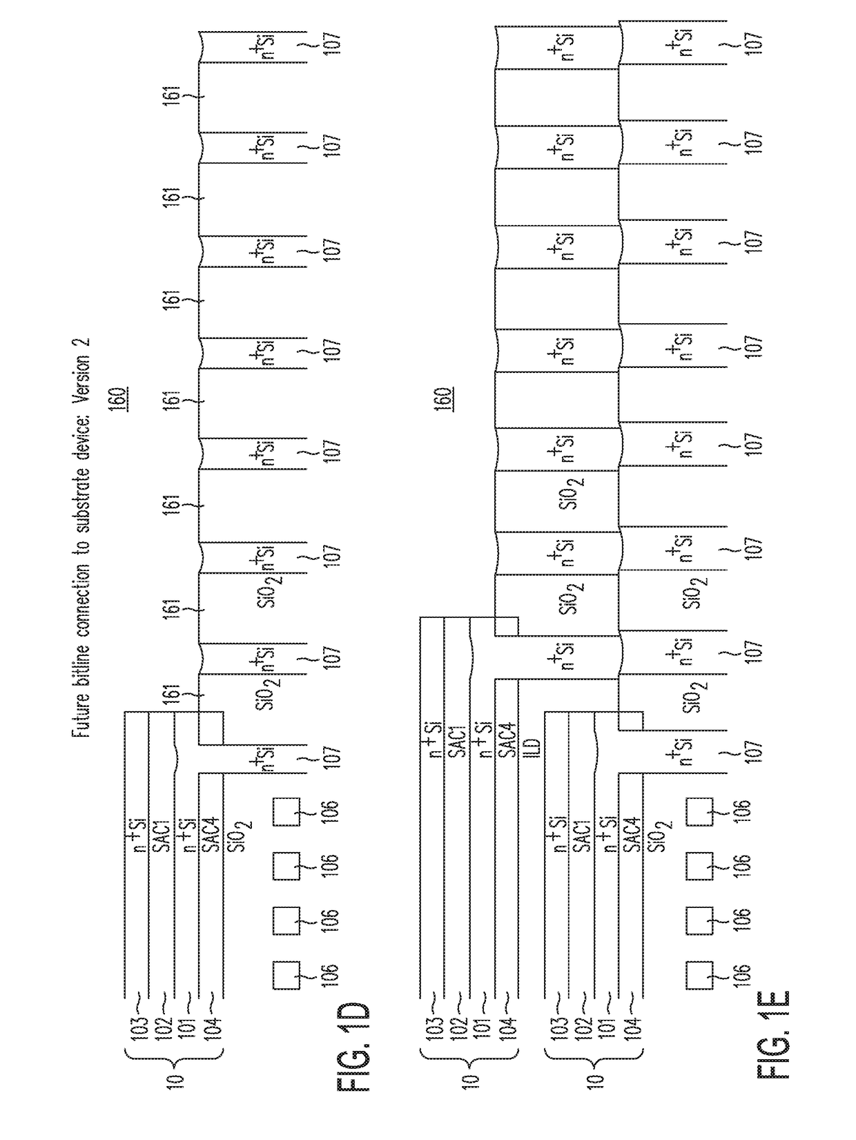
[0104]In this embodiment, the SAC4 material-containing sublayer or sublayers (e.g., second sacrificial sublayers 304a and 304b of FIG. 7), are removed by etching long cavities in the direction along the length each sublayer, instead of side-ways (i.e., in the direction along its width) through exposed portions from side walls of the trenches, as was shown above in conjunction with FIGS. 6-7 (Embodiment 1) above. In other words, etchant sequentially removes SAC4 material from one or both ends along the length of the second sacrificial sublayer or sublayers. While this etch takes longer paths, Embodiment 2 has an advantage over Embodiment 1 in that metal replacement may be carried out after the memory cells have been formed, thereby reducing the risk of metal contamination in the memory cells.

[0105]FIG. 13 shows memory structure 400 that is substantially the same as the memory structure 300 of FIG. 11, except for removal of second sacrificial sublayers 304a and 304b and metal replacem...

embodiment 3

[0111]Alternatively, the NIN stacks can be built incrementally in two or more portions. In each portion, only a limited number of active layers are etched in the vertical direction. Specifically, etching of high aspect ratio NIN stacks are avoided in the initial portion (portion 1) by etching fewer active layers, which reduces the aspect ratio. When a subsequent portion of the NIN stacks is added on top of an earlier portion of the NIN stacks and etched, the earlier portion is supported by a dielectric layer that is deposited in the trenches of the earlier portion. The subsequent portion is self-supporting during its etch, as the etch does not create a high aspect ratio structure. When all the portions of the NIN stacks have been fabricated, a dielectric layer is deposited to fill any remaining open trenches, patterned, and etched to remove all previously deposited like dielectric layers from all earlier portions of the NIN stacks, while maintaining the mechanical strength of the NI...


PUM

PropertyMeasurementUnit
thicknessaaaaaaaaaa
thicknessaaaaaaaaaa
aspect ratioaaaaaaaaaa

Abstract

A method addresses low cost, low resistance metal interconnects and mechanical stability in a high aspect ratio structure. According to the various implementations disclosed herein, a replacement metal process, which defers the need for a metal etching step in the fabrication process until after all patterned photoresist is no longer present. Under this process, the conductive sublayers may be both thick and numerous. The present invention also provides for a strut structure which facilitates etching steps on high aspect ratio structures, which enhances mechanical stability in a high aspect ratio memory stack

Description

CROSS REFERENCES TO RELATED APPLICATIONS[0001]This application is related to copending U.S. patent application (“Copending Application”), Ser. No. 15 / 248,420, entitled “Capacitive-Coupled Non-Volatile Thin-film Transistor Strings in Three-Dimensional Arrays,” filed Aug. 26, 2016. The Copending Application is hereby incorporated by reference in its entirety. The Copending Application has been published as U.S. 2017 / 0092371. References to the Copending Application herein are made by paragraph numbers of the publication. The present application is also related to and claims priority of: (i) U.S. provisional application (“Provisional Application I”), Ser. No. 62 / 522,666, entitled “Replacement Metal and Strut for 3D memory Array,” filed on Jun. 20, 2017: U.S. provisional application (“Provisional Application II”), Ser. No. 62 / 522,661, entitled “3-Dimensional NOR String Arrays in Segmented Stacks,” filed on Jun. 20, 2017; (iii) U.S. provisional application (“Provisional Application III”),...

Claims


Application Information

Patent Timeline
Patent Type & Authority Applications(United States)
IPC IPC(8): H01L27/11582H01L21/768H01L23/00H01L21/311
CPCH01L27/11582H01L21/76802H01L23/562H01L21/7682H01L21/31111G11C16/0466H10B43/27H10B43/20
Inventor HARARI, ELIHERNER, SCOTT BRADCHIEN, WU-YI
Owner SUNRISE MEMORY CORP
Why Eureka
Try Eureka