Semiconductor device and production method

a technology of semiconductor devices and production methods, applied in semiconductor devices, diodes, radiation controlled devices, etc., can solve the problems of reducing an impurity concentration, affecting the production efficiency of semiconductor devices, and affecting the quality of semiconductor devices, so as to prevent the degradation of noise characteristics

Active Publication Date: 2018-12-27
SONY CORP
View PDF4 Cites 0 Cited by
  • Summary
  • Abstract
  • Description
  • Claims
  • Application Information

AI Technical Summary

Benefits of technology

[0028]In one aspect of the present technology, the degradation of the noise characteristics can be prevented.
[0029]Note that the effect described herein is not necessarily restrictive, but may be one of the effects described in the present disclosure.

Problems solved by technology

Such a general MOS transistor formed in a semiconductor device or an imaging device, particularly the surface channel MOS transistor in which a channel region is formed on a surface side of the semiconductor substrate, has a possibility that mobility and noise characteristics degrade due to a carrier trap that exists in the vicinity of an interface between the semiconductor substrate and a gate insulating film.
However, an impurity whose ion is implanted in the channel region causes decrease of an impurity concentration due to segregation, pileup, diffusion, and the like of the impurity on an element separating region side of the channel region, because of influence of a heat process.
Thereby, there is a possibility that the noise characteristics degrade due to reduction in the effective gate width.

Method used


Image

  • Semiconductor device and production method
  • Semiconductor device and production method
  • Semiconductor device and production method

Examples


application example

6. Application Example to Electronic Device

7. Usage Example

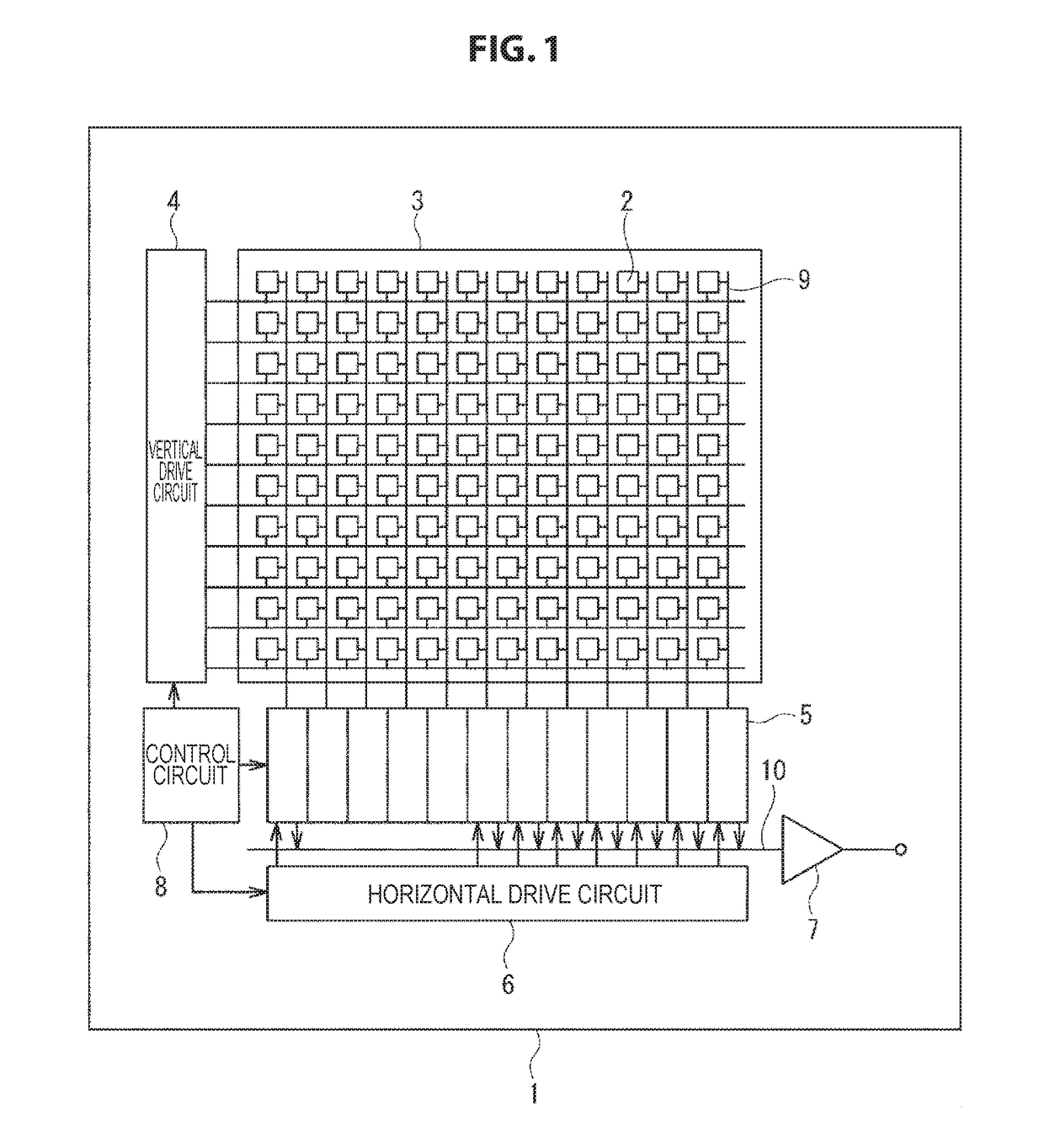
[0048]FIG. 1 is a diagram illustrating a configuration of one embodiment of an imaging device that employs the present technology. The imaging device 1 in the present embodiment includes a pixel region 3 composed of a plurality of pixels 2 arrayed on a substrate made of silicon, a vertical drive circuit 4, column signal processing circuits 5, a horizontal drive circuit 6, an output circuit 7, a control circuit 8, etc.

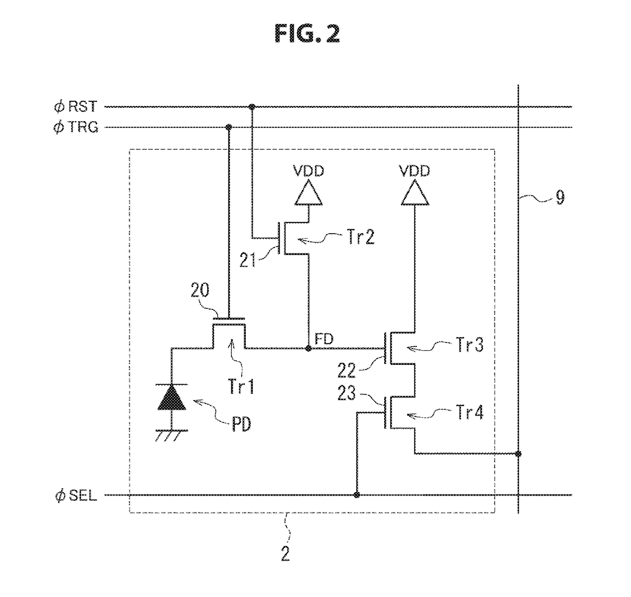
[0049]The pixel 2 is configured with a photoelectric conversion unit including a photo diode and a plurality of pixel transistors, and a plurality of pixels 2 are arranged regularly in a two-dimensional array on the substrate. The pixel transistors that configures the pixel 2 may be four MOS transistors including a transfer transistor, a reset transistor, a selection transistor, and an amplifier transistor, and may be three transistors excluding the selection transistor. The present embodiment employs an example...


PUM


Abstract

The present technology relates to a semiconductor device and a production method that enable noise reduction. A drain region and a source region provided in a predetermined region of a semiconductor substrate; a channel region provided between the drain region and the source region; and a gate electrode formed on the channel region are included. The channel region includes a first impurity diffusion region, and a second impurity diffusion region that is an impurity diffusion region of a same conductivity type as the first impurity diffusion region, and has an impurity concentration different from an impurity concentration of the first impurity diffusion region, and is formed at a substantially center part of the first impurity diffusion region. The present technology can be applied to a transistor that configures an imaging device, for example.

Description

TECHNICAL FIELD[0001]The present technology relates to a semiconductor device and a production method. Its detail relates to a semiconductor device and a production method that can prevent generation of noise.BACKGROUND ART[0002]In the past, a general MOS transistor formed in a semiconductor device or an imaging device is a surface channel type in which a region under a gate electrode is formed of an impurity region of an opposite conductivity type to a source-drain region. In the surface channel MOS transistor, a channel formed of an inversion layer is formed on a semiconductor substrate surface by applying voltage to the gate electrode, in order to flow electric current between a source and a drain.[0003]Such a general MOS transistor formed in a semiconductor device or an imaging device, particularly the surface channel MOS transistor in which a channel region is formed on a surface side of the semiconductor substrate, has a possibility that mobility and noise characteristics degr...

Claims


Application Information

Patent Timeline
Patent Type & Authority Applications(United States)
IPC IPC(8): H01L27/146H01L21/266H01L21/265
CPCH01L27/14616H01L27/14643H01L27/14689H01L21/266H01L21/26513H01L29/78H01L29/1045H01L27/146H01L21/822H01L21/8234H01L27/04H01L27/06H01L27/08H01L27/088
Inventor TONEGAWA, SUSUMU
Owner SONY CORP
Why Eureka
Try Eureka