

Exposure apparatus, control method for the same, and device manufacturing method
a technology of exposure apparatus and control method, which is applied in the direction of lighting and heating apparatus, printing, instruments, etc., can solve the problems of reducing throughput, degrading the performance of the optical element, and unable to achieve conventional photolithography arrangements employing ultraviolet light, so as to prolong the service life of the optical element and prevent the degradation of the optical element
- Summary
- Abstract
- Description
- Claims
- Application Information
AI Technical Summary
Benefits of technology
Problems solved by technology
Method used
Image

Examples
Embodiment Construction
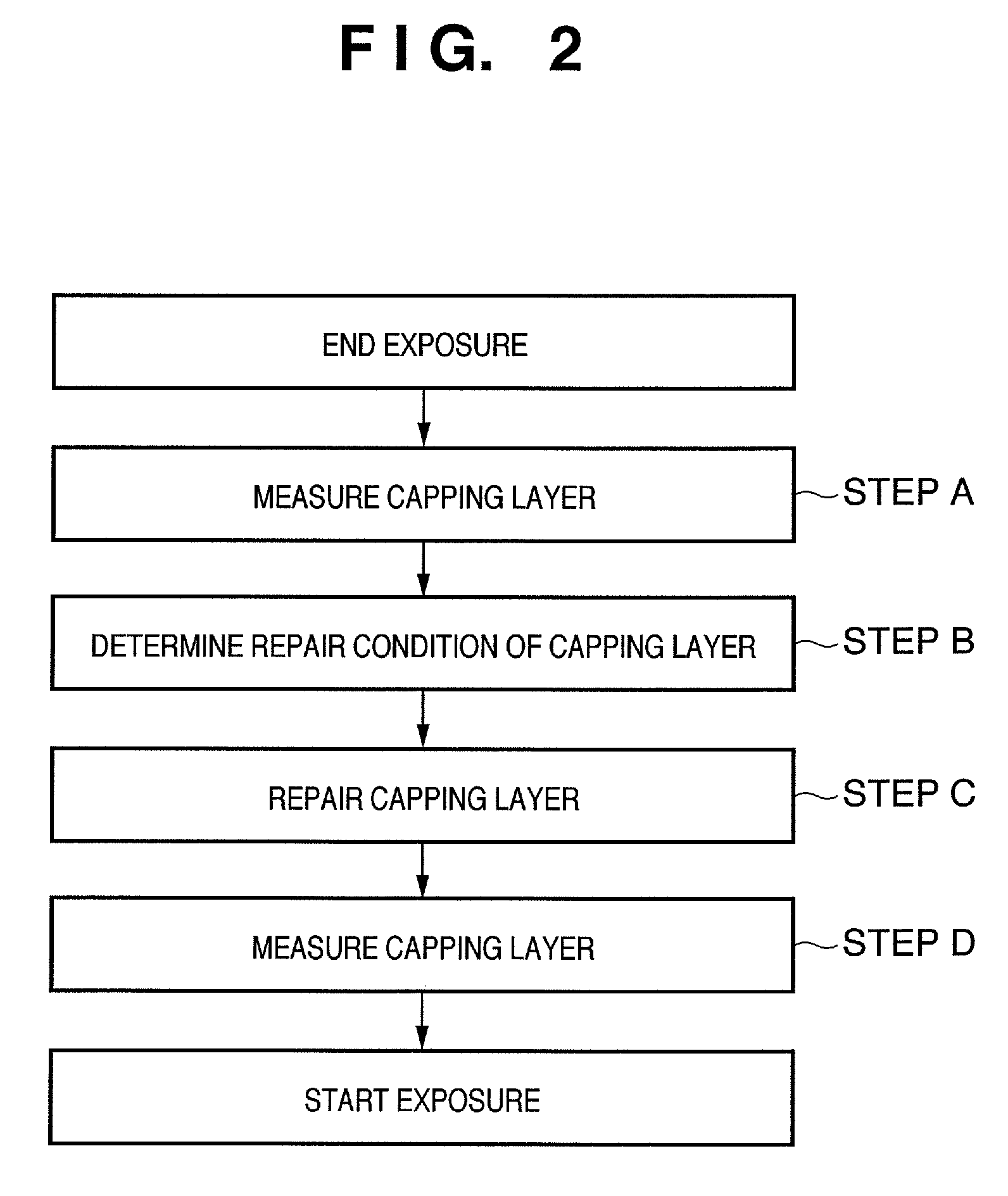
[0042]Preferred embodiments of the present invention will be described with reference to the accompanying drawings. In the drawings, the same reference numerals denote the same members.
[0043]An exposure apparatus according to the present invention is suitable, in the manufacturing process of, e.g., a semiconductor device, such as an LSI or CCD, an LCD, a magnetic sensor, and a thin film magnetic head, to transfer a pattern on an original onto a substrate coated with a photosensitive agent with exposure light.
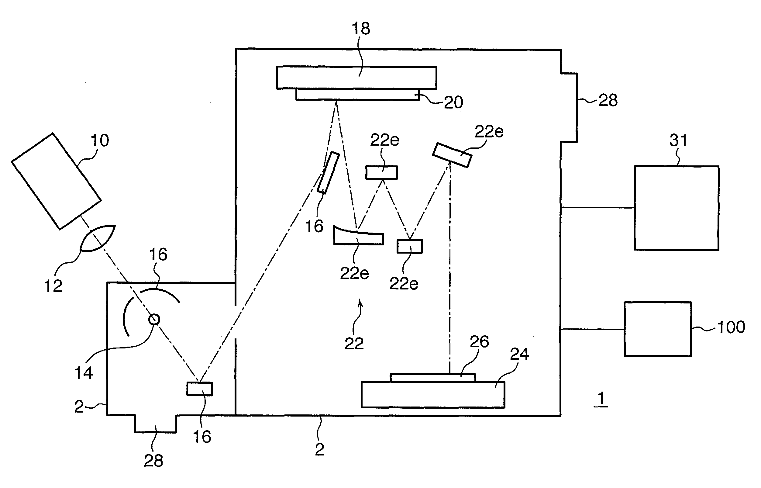
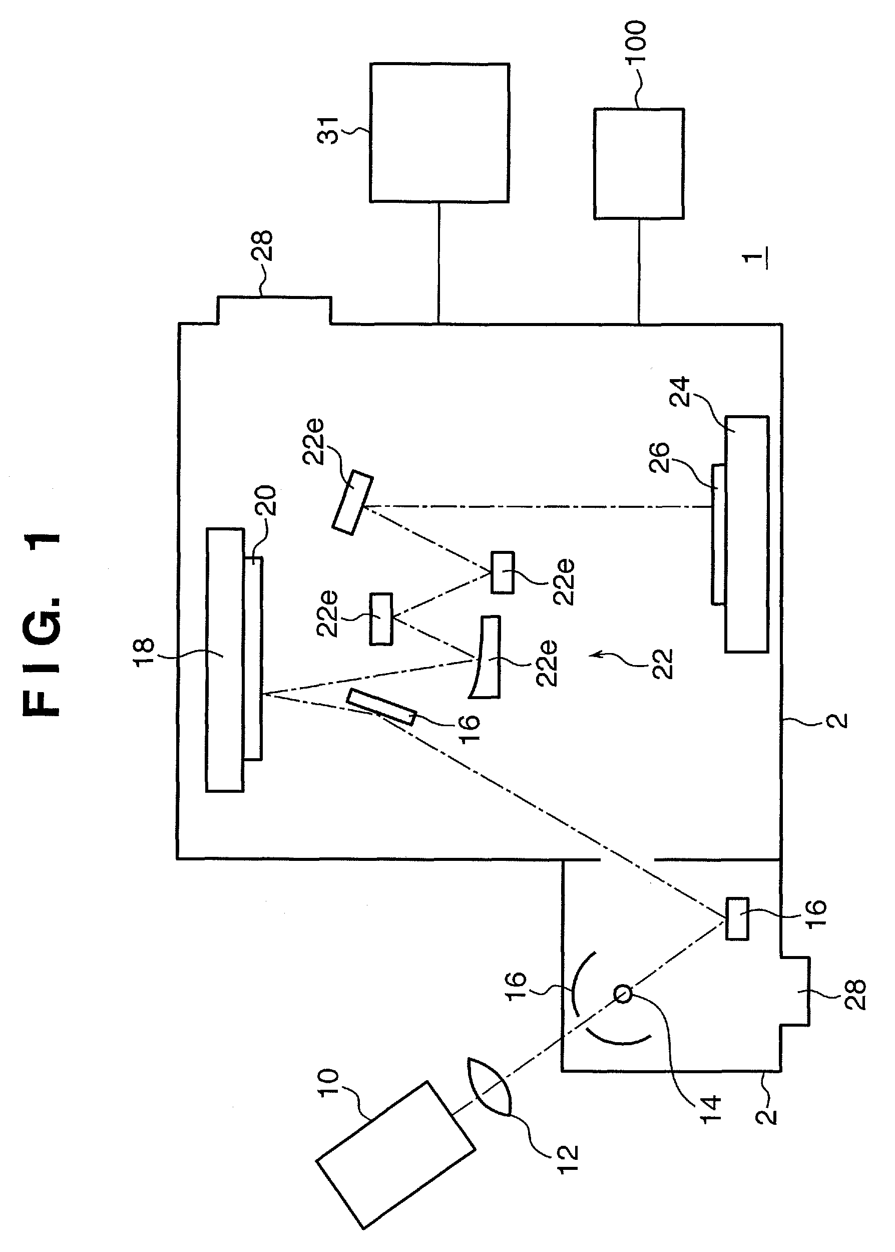
[0044]An exposure apparatus according to a preferred embodiment of the present invention will be described. FIG. 1 is a view schematically showing an example of the overall arrangement of an EUV exposure apparatus according to a preferred embodiment of the present invention. An EUV exposure apparatus 1 comprises a vacuum chamber 2 in which one or a plurality of optical elements each having a capping layer are arranged, and which exposes a substrate by using the optical elements....
PUM
 Abstract
Description
Claims
Application Information