

Interface Charge Reduction for SiGe Surface
- Summary
- Abstract
- Description
- Claims
- Application Information
AI Technical Summary
Benefits of technology
Problems solved by technology
Method used
Image

Examples
Embodiment Construction
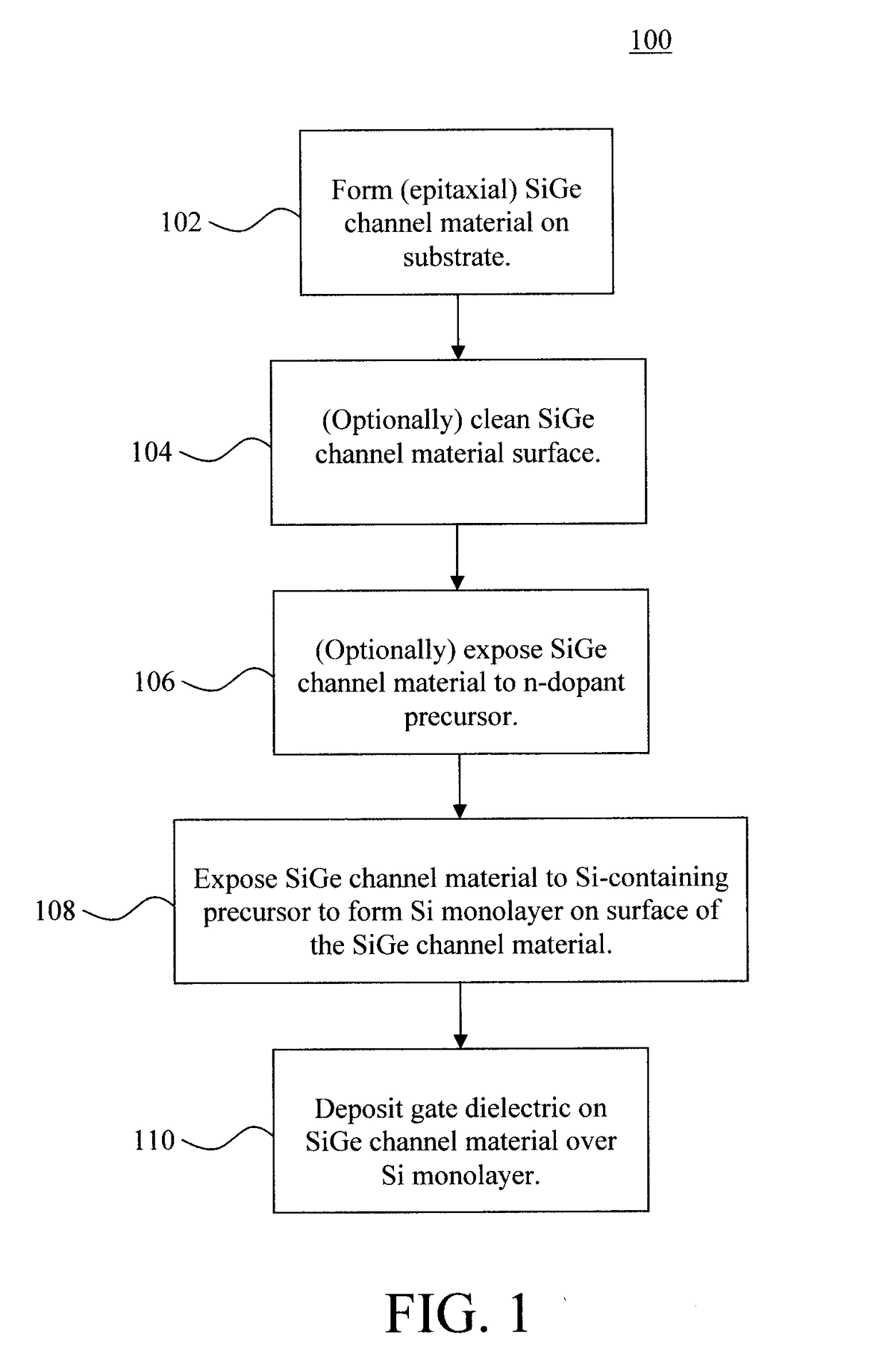
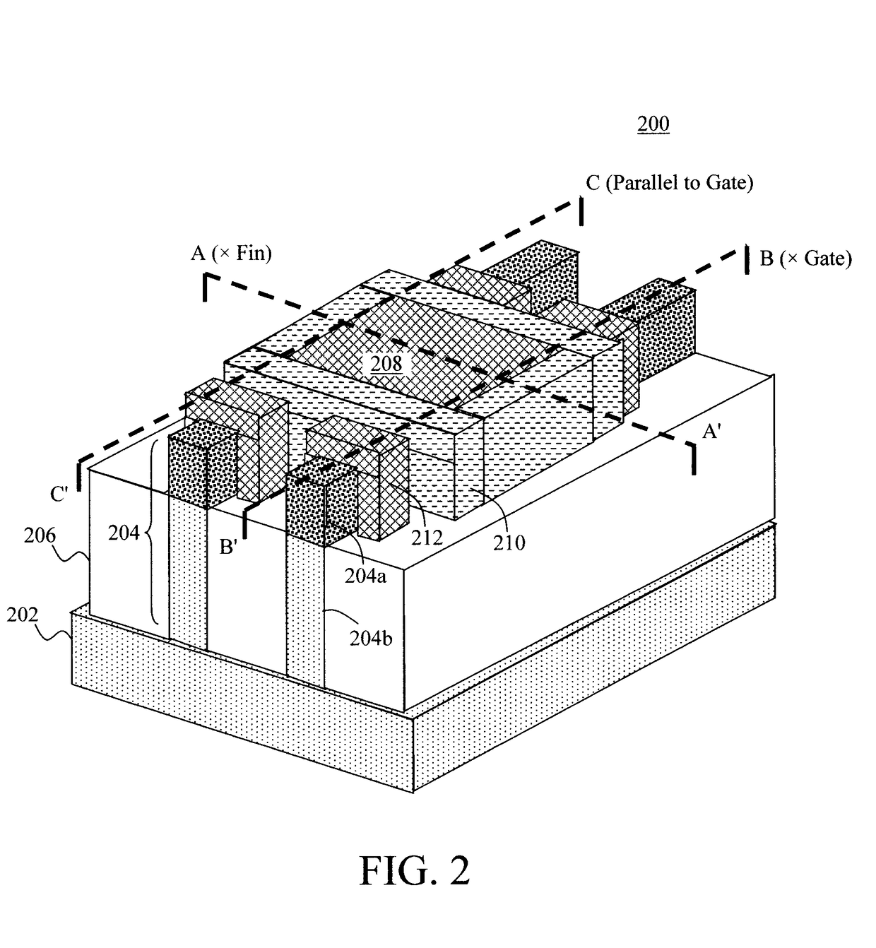
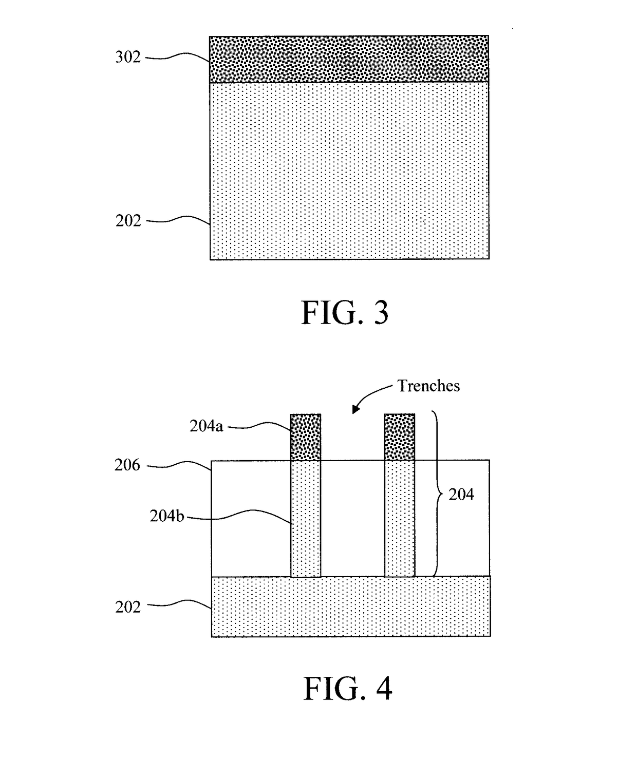
[0027]Provided herein are techniques for reducing interface charge density (Dit) at the gate dielectric for silicon germanium (SiGe) channel-based devices. As will be described in detail below, the present techniques involve, prior to placing the gate dielectric, exposing the surface(s) of the SiGe channel to a silicon (Si)-containing chemical precursor (such as dichlorosilane SiH2Cl2 (DCS)) to grow a nominally continuous thin. Si (e.g., less than 5 monolayers thick) on the SiGe to passivate the SiGe / gate dielectric interface and significantly reduce the Dit. Prior to exposure to the Si-containing chemical precursor, the SiGe channel can be exposed to an n-dopant precursor (such as phosphine) of a variable concentration to dope the SiGe with an n-type dopant. Advantageously, all of these processes can be performed in-situ following (epitaxial) growth of the SiGe, and can be easily integrated into different device process flows. When reference is made herein to ‘monolayer’ or ‘monola...
PUM
 Abstract
Description
Claims
Application Information