Gate-all-around field-effect-transistor devices and fabrication methods thereof

a technology of effect transistor and gate-all-around, which is applied in the direction of semiconductor devices, electrical equipment, nanotechnology, etc., can solve the problems of affecting the electrical performance of the fet, the fabrication process of gaa fets becomes more and more difficult, and the performance of the gaa fets may be degraded

Active Publication Date: 2019-02-14
SEMICON MFG INT (SHANGHAI) CORP +1
View PDF3 Cites 13 Cited by
  • Summary
  • Abstract
  • Description
  • Claims
  • Application Information

AI Technical Summary

Benefits of technology

[0007]One aspect of the present disclosure provides a method for fabricating a gate-all-around (GAA) field-effect-transistor (FET) device. The method includes providing a base substrate and forming a plurality of first stacked structures on the base substrate. Each first stacked structure includes a first sacrificial layer and a first semiconductor layer formed on the first sacrificial layer. The method includes forming a first dummy gate structure across the plurality of first stacked structures, and a first sidewall spacer on each sidewall surface of the first dummy gate structure. The first dummy gate structure is formed on a portion of the base substrate and covers a portion of a top surface and a portion of each sidewall surface of the plurality of first stacked structures. The method includes forming a first source/drain doped layer in the plurality of first stacked structures on each side of the first dummy

Problems solved by technology

As the size of traditional planar transistors is continuously reduced, the ability of traditional planar transistors in controlling the channel currents becomes weaker, resulting in the short-channel effect (SCE) and causing leakage currents, which ultimately affect the electrical performance of the FETs.
However, as the density of GAA FETs increases and the size shrinks, the fabrication process for GAA FETs be

Method used


Image

  • Gate-all-around field-effect-transistor devices and fabrication methods thereof
  • Gate-all-around field-effect-transistor devices and fabrication methods thereof
  • Gate-all-around field-effect-transistor devices and fabrication methods thereof

Examples


Embodiment Construction

[0014]Reference will now be made in detail to exemplary embodiments of the invention, which are illustrated in the accompanying drawings. Wherever possible, the same reference numbers will be used throughout the drawings to refer to the same or like parts.

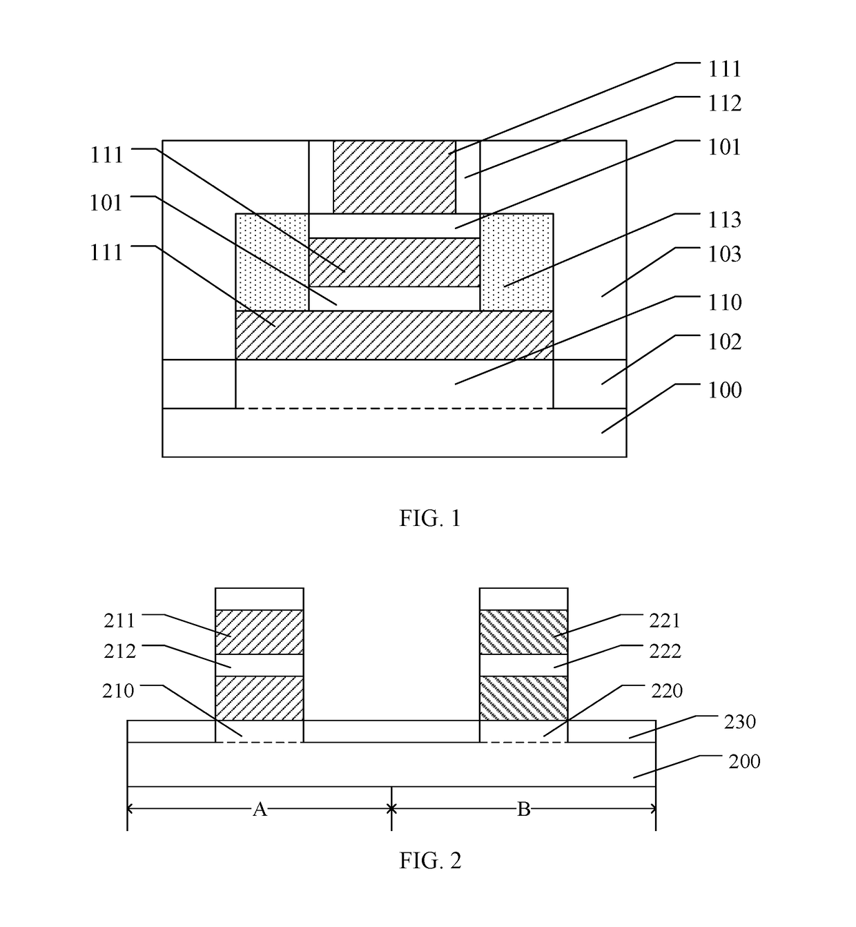
[0015]FIG. 1 illustrates a schematic cross-section view of a gate-all-around (GAA) field-effect-transistor (FET) device. Referring to FIG. 1, the GAA FET device includes a substrate 100, a fin structure 110 formed on the substrate 100, and a plurality of stacked semiconductor structures (not labeled) formed on the fin structure 110. Each stacked semiconductor structure includes a semiconductor layer 101 and a via (not shown) under the semiconductor layer 101. That is, the GAA FET device includes a plurality of semiconductor layers 101 and a plurality of via alternately disposed on the fin structure 110.

[0016]The GAA FET device also includes an isolation structure 102 formed on the substrate 100 and covering the sidewall surfaces of...


PUM


Abstract

A method for fabricating a gate-all-around field-effect-transistor device includes forming a plurality of first stacked structures, each including a first sacrificial layer and a first semiconductor layer; forming a first dummy gate structure across the first stacked structures and partially covering the top and the sidewall surfaces of each first stacked structure, and a first sidewall spacer on each sidewall surface of the first dummy gate structures; forming a first source/drain doped layer, and a dielectric structure exposing the top surfaces of the first dummy gate structure and each first sidewall spacer; removing the first dummy gate structure to form a first trench; removing a portion of the first sacrificial layer to form a first via which partially exposes the first source/drain doped layer; forming a first barrier layer on the first source/drain doped layer; and forming a first gate structure to fill the first trench and the first via.

Description

CROSS-REFERENCES TO RELATED APPLICATIONS[0001]This application claims the priority of Chinese Patent Application No. CN201710671276.6, filed on Aug. 8, 2017, the entire content of which is incorporated herein by reference.FIELD OF THE DISCLOSURE[0002]The present disclosure generally relates to the field of semiconductor fabrication technology and, more particularly, relates to gate-all-around field-effect-transistor devices and fabrication methods thereof.BACKGROUND[0003]With the rapid development of semiconductor manufacturing technology, field-effect-transistors (FETs) have been developed toward a direction of having a higher component density and a higher integration level, and the gate size of planar transistors has also become smaller and smaller. As the size of traditional planar transistors is continuously reduced, the ability of traditional planar transistors in controlling the channel currents becomes weaker, resulting in the short-channel effect (SCE) and causing leakage c...

Claims


Application Information

Patent Timeline
IPC IPC(8): H01L29/423H01L29/66H01L29/08H01L21/02H01L21/311H01L29/36H01L21/265H01L29/06H01L29/78
CPCH01L29/42392H01L29/66545H01L29/0847H01L29/6656H01L29/66795H01L21/0214H01L21/31111H01L29/36H01L21/26513H01L21/0262H01L21/02164H01L29/0673H01L29/785H01L29/165H01L29/7848H01L21/32135H01L21/31116H01L29/1033H01L29/4236H01L29/66477H01L29/78H01L29/78696H01L29/66742H01L29/78681H01L29/78684B82Y10/00H01L29/401H01L29/66439H01L29/775
Inventor ZHOU, FEI
Owner SEMICON MFG INT (SHANGHAI) CORP
Why Eureka
Try Eureka